Executive Takeaways
- The $10B Catalyst: SEMICON India 2026 serves as the definitive global showcase for India’s semiconductor mission, drawing over $15 billion in committed capital allocations and enterprise joint ventures.
- Indigenous AI Silicon: Domestic innovators like Netrasemi are scaling mass production of advanced hardware, highlighted by the commercial rollout of the A2000 AI chip.
- Automotive & Industrial Pivots: Tier-1 consulting and engineering giants, including Tata Consultancy Services (TCS), are deploying proprietary custom chip designs tailored specifically for next-generation automotive architecture.
- Global Supply Chain Diversification: Multinational foundries and OSAT (Outsourced Semiconductor Assembly and Test) providers are accelerating infrastructure scalability across Gujarat, Karnataka, and Tamil Nadu to mitigate geopolitical risk.
NEW DELHI — In the cavernous exhibition halls of the capital, a quiet revolution has found its loudest megaphone. SEMICON India 2026 has officially redefined the global technology discourse, transforming what was once dismissed as an ambitious geopolitical aspiration into a hard-coded industrial reality. As international executives, venture capitalists, and policy architects converge on New Delhi, the underlying narrative is unmistakable: India is no longer merely a consumer or software back-office of the global semiconductor ecosystem. It is aggressively constructing the foundational infrastructure of the next silicon century.
Reporting from New Delhi, the current landscape captured by industry watchers points to a structural shift in capital allocation, valuation multiples, and cross-border supply chain dependencies. With the global chip architecture facing persistent vulnerabilities, soaring enterprise ROI demands, and escalating regulatory compliance pressures across traditional manufacturing hubs, India’s emergence as a viable, subsidized, and talent-rich alternative has shifted from a theoretical exercise to a boardroom imperative.
The Genesis of India's Silicon Ambition: Catalyzing the Ecosystem
To understand the gravity of SEMICON India 2026, one must examine the rapid maturation of the domestic landscape over the preceding 36 months. When the central government initially rolled out its multi-billion-dollar Production Linked Incentive (PLI) schemes, skeptics pointed to historical hurdles: water and power intensity, exorbitant capital expenditures, and an acute shortage of domestic fabrication (fab) engineering talent.
Those criticisms, while valid in 2022, have been systematically dismantled through aggressive public-private partnerships, streamlined regulatory compliance, and targeted educational initiatives. Groundbreakings in states like Gujarat and Karnataka have evolved into active construction sites, where cleanrooms and lithography infrastructure are rising at unprecedented velocity. The overarching market liquidity flowing into Indian semiconductor startups and design houses has fundamentally altered venture capital dynamics across South Asia.
Furthermore, the domestic market’s insatiable appetite for localized compute architecture—driven by the rapid expansion of sovereign AI initiatives, hyper-scale cloud data centers, and an exploding electric vehicle (EV) sector—has provided an immediate, de-risked customer base for early-stage chip designers.
Domestic Innovation in Action: Netrasemi’s A2000 and TCS Custom Silicon
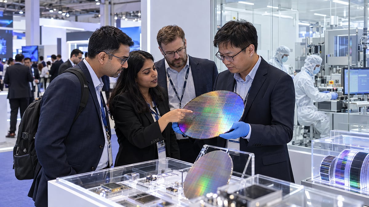
The credibility of India’s semiconductor push was underscored months prior to the conference when Netrasemi announced its landmark timeline to mass-produce the A2000 AI chip. Designed to handle intensive edge-AI workloads, real-time computer vision, and industrial automation data streams, the A2000 represents a watershed moment for domestic fabless semiconductor design. By targeting high-efficiency, low-power enterprise deployment, Netrasemi has proven that Indian firms can successfully navigate the brutal unit economics and rigorous verification cycles of complex System-on-Chip (SoC) development.
Concurrently, enterprise behemoths are entering the fray with institutional force. Tata Consultancy Services (TCS) used the shadow of SEMICON India 2026 to showcase its proprietary custom chip design capabilities targeted squarely at the automotive and industrial sectors. As modern vehicles evolve into data centers on wheels—requiring millions of lines of code and dedicated neural processing units—automakers are demanding custom silicon to optimize power management, latency, and thermal efficiency. TCS’s entry into custom chip design bridges the gap between enterprise software prowess and hardware realization, offering global OEMs a vertically integrated design partner.
| Metric / Milestone | 2024 Baseline | SEMICON India 2026 Status | Strategic Implication |
|---|---|---|---|
| Committed Capital Inflows | ~$6.5 Billion | Exceeding $15 Billion | Accelerated infrastructure scalability across OSAT and Fab projects. |
| Domestic AI Silicon Production | Proof-of-Concept / FPGA | Mass Production (e.g., Netrasemi A2000) | Reduction of import dependency for edge-AI infrastructure. |
| Automotive Chip Integration | Imported Microcontrollers | TCS Custom Silicon Solutions | Enhanced margins and supply chain security for EV manufacturers. |
| Design Talent Pool | ~50,000 Engineers | ~120,000+ Specialized Engineers | Global R&D migration to Indian design centers. |
Industry & Market Implications: Who Wins, Who Loses
The structural transformation highlighted at SEMICON India 2026 carries profound implications for global asset allocators and supply chain strategists. The traditional hegemony held by East Asian manufacturing hubs is facing its most credible diversification test to date.
The Winners
- Fabless Startups & Domestic Design Houses: Access to venture capital, government co-funding, and local testing facilities has vastly shortened time-to-market for Indian chip designers.
- Global Equipment & EDA Vendors: Applied Materials, Synopsys, Cadence, and ASML ecosystem players are seeing exponential revenue growth as Indian entities build out greenfield R&D and manufacturing labs.
- Automotive & Industrial OEMs: Vehicle manufacturers operating in India gain a localized hedge against global shipping bottlenecks, foreign exchange volatility, and geopolitical trade restrictions.
The Vulnerabilities & Structural Risks
Despite the palpable optimism, risk mitigation remains a central theme for institutional investors. Raw material dependencies, particularly for ultra-pure electronic gases, specialized chemicals, and silicon wafers, still require robust import channels. Furthermore, while India boasts a massive reservoir of digital design talent, specialized process engineering and lithography floor-operation expertise require sustained, multi-year vocational scaling to meet global standards.
Frequently Asked Questions (People Also Ask)
What is the primary objective of SEMICON India 2026?
SEMICON India 2026 serves as the premier international platform to showcase India's semiconductor manufacturing, design, and packaging advancements. Its goal is to foster global partnerships, attract foreign direct investment (FDI), and solidify the nation's position as a reliable pillar in the global semiconductor supply chain.
How is Netrasemi contributing to India’s semiconductor growth?
Netrasemi is spearheading commercial domestic hardware innovation by initiating mass production of its advanced A2000 AI chip this year. The chip targets high-performance edge-AI, industrial IoT, and computer vision applications, validating India’s capability to design and manufacture complex silicon locally.
What role are IT giants like TCS playing in the semiconductor boom?
Companies like Tata Consultancy Services (TCS) are expanding beyond traditional software services into hardware engineering, launching custom chip design solutions tailored specifically for the automotive, industrial, and telecommunications sectors. This bridges the critical gap between software architecture and bespoke physical silicon.
Which regions in India are emerging as semiconductor hubs?
Gujarat, Karnataka, Tamil Nadu, and Uttar Pradesh are rapidly scaling into primary semiconductor clusters, driven by state-level incentive packages, robust academic institutions, reliable power infrastructure, and proximity to major electronics manufacturing ecosystems.
Future Outlook: Milestones to Watch
As the curtains close on SEMICON India 2026, the real test shifts from conference declarations to execution metrics. Over the next 18 to 24 markets, financial analysts and industry stakeholders will closely monitor several key performance indicators:
- First-Silicon Tape-Outs: The successful fabrication and yield validation of complex domestic enterprise and AI chips rolling out of newly established Indian foundries and OSAT facilities.
- Pipeline Conversion: The conversion of MOU-stage foreign investments into operational capital expenditures on Indian soil.
- Workforce Scalability: The output volume of specialized semiconductor packaging and fabrication engineers graduating from newly minted academic-industrial training partnerships.
India’s chip ambitions are no longer a distant macroeconomic hypothesis. As evidenced by the innovations on display in New Delhi, the foundation has been poured, the capital is deployed, and the silicon age in South Asia has officially begun.