The Silicon Pivot: Inside Micron’s $2.75 Billion Gujarat Gambit and the Rewiring of the Global Chip Axis
Executive Takeaways
- Historic Milestone: Micron Technology has officially commenced commercial operations at its Assembly, Test, Marking, and Packaging (ATMP) facility in Sanand, Gujarat, marking the operationalization of India’s first major commercial-scale semiconductor production node.
- Asymmetrical Capital Engineering: The landmark $2.75 billion project reflects a unique public-private capital structure, with Micron deploying approximately $825 million in balance-sheet equity, leveraged against a 70% aggregate fiscal subsidy package funded by the central Indian government and the state of Gujarat.
- AI Memory Bottleneck Mitigation: The facility primarily processes high-performance Dynamic Random-Access Memory (DRAM) and NAND flash memory wafers, addressing mission-critical back-end bottlenecks for artificial intelligence (AI) servers, autonomous mobility, and hyperscale cloud infrastructure.
- Geostrategic Supply Chain De-risking: The Sanand plant operationalizes a tangible "China+1" and "Taiwan Hedge" hedge for global tech hardware, fundamentally transforming India from a pure-play silicon design hub into an active hardware manufacturing jurisdiction.
The Sanand Breakthrough: Rewriting the Semiconductor Geopolitical Order

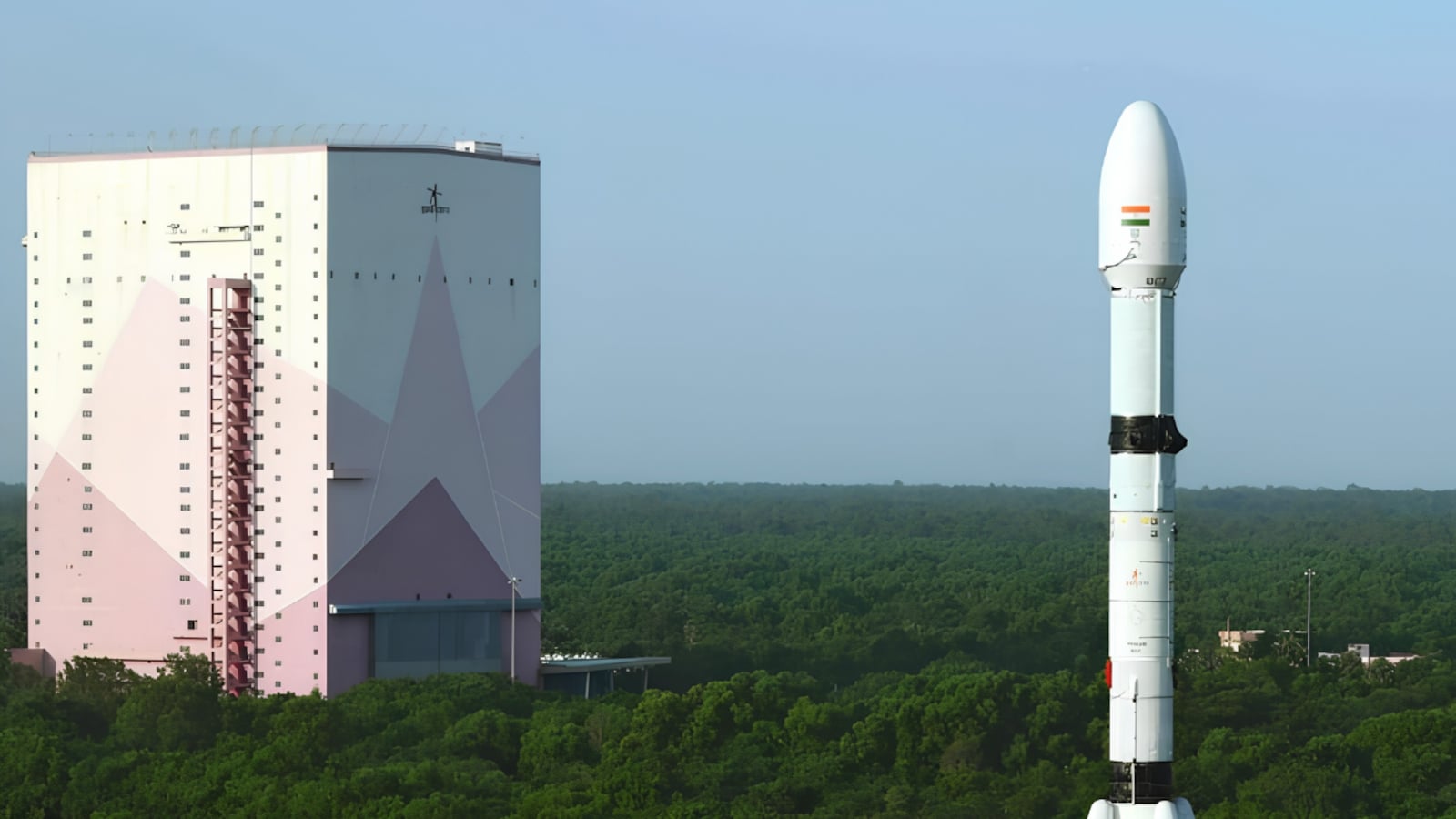
In the industrial expanse of Sanand, Gujarat—historically known as an automotive corridor—a high-stakes geopolitical experiment has crossed into commercial reality. Micron Technology Inc. has officially operationalized India's first world-class semiconductor assembly and test facility. The inauguration represents far more than an operational expansion for the Boise, Idaho-based memory titan; it serves as the definitive stress test for the Indian government’s $10 billion India Semiconductor Mission (ISM) and signals a critical inflection point in the diversification of the global technology supply chain.
For decades, the global semiconductor architecture has operated on a hyper-concentrated, razor-thin equilibrium. Front-end wafer fabrication has remained tethered to Taiwan, South Korea, and Japan, while back-end assembly, packaging, and testing (OSAT/ATMP) consolidated within mainland China, Malaysia, and Southeast Asian enclaves. However, mounting cross-strait geopolitical friction, post-pandemic supply vulnerabilities, and the explosive compute demands of the generative AI paradigm have forced institutional capital and enterprise boardrooms to aggressively pursue radical supply chain resilience.
Micron’s Sanand project represents the leading edge of this capital redeployment. Spanning over 500,000 square feet of ultra-pure cleanroom environment in its initial phase, the site is designed to process advanced silicon wafers fabricated at Micron’s global foundries into packaged modules ready for integration into enterprise hardware. As modern server architectures require unprecedented densities of DRAM and high-layer 3D NAND to feed latency-sensitive AI model weights, the commissioning of Sanand directly links the Indian subcontinent to the highest-margin sectors of enterprise cloud infrastructure.
Capital Allocation Breakdown: The 70% Subsidy Architecture
The financial engineering underlying the Sanand facility represents one of the most generous sovereign subsidy frameworks in contemporary industrial policy. The total project capitalization stands at $2.75 billion, bifurcated across two distinct operational phases. Yet, under the terms framed by the India Semiconductor Mission and Gujarat’s state-level electronics manufacturing policies, Micron’s direct corporate capital expenditure is strictly capped at approximately $825 million.
The remaining 70% of the capital expenditure is state-underwritten: the central government of India provides 50% of the total project cost on a pari-passu basis, while the Gujarat state administration injects an additional 20% through infrastructure subsidies, subsidized land allocation, high-voltage power guarantees, and long-term utility concessions. This radical capital subsidization dramatically lowers Micron’s weighted average cost of capital (WACC) and insulates the chipmaker’s balance sheet against short-term memory cycle drawdowns, while guaranteeing rapid enterprise return on investment (ROI).
For New Delhi, the financial asymmetry is an intentional loss-leader. Prime Minister Narendra Modi’s administration has consistently recognized that leading-edge, multi-billion-dollar wafer foundries will not risk greenfield expansion in emerging markets without an existing domestic ecosystem of chemical suppliers, specialized industrial gas providers, precision substrate handlers, and an experienced cleanroom labor force. By underwriting Micron’s back-end facility, the Indian government has effectively purchased the operational nucleus around which an entire domestic semiconductor cluster can now coalesce.
Technical Architecture: From Raw Wafers to AI-Ready Silicon
The operational scope of the Sanand site centers on assembly, testing, marking, and packaging (ATMP). While front-end fabrication—the printing of integrated circuits onto raw silicon wafers via extreme ultraviolet (EUV) and deep ultraviolet (DUV) photolithography—remains concentrated in capital-intensive mega-fabs across the United States, Japan, and Taiwan, back-end packaging has evolved far beyond legacy, low-tech wire bonding.
In modern high-performance computing (HPC), back-end packaging dictates thermal performance, form factor, and interconnect bandwidth. The Sanand plant receives processed 300mm DRAM and NAND wafers from Micron’s global fabrication footprint. Within the facility’s Class 100 and Class 1,000 cleanroom environments, automated diamond-blade saws and laser-dicing apparatus slice wafers into microscopic, individual dies. These dies are subsequently processed using Ball Grid Array (BGA) architectures, multi-chip packaging (MCP), and advanced flip-chip interconnect methodologies.
The facility’s secondary core function is automated test engineering. With enterprise customers demanding six-sigma reliability metrics for mission-critical data center deployments, the Sanand campus deploys custom high-speed automated test equipment (ATE) to subject packaged memory modules to extreme thermal variation, structural vibration, and electrical stress-testing under simulated production workloads. The resulting output spans enterprise-grade solid-state drives (SSDs), low-power double data rate (LPDDR5X) modules tailored for AI-integrated smartphones, and high-density memory packages powering next-generation server clusters.
Verified Structural & Operational Metrics
The following audited operational data outlines the financial, physical, and technical footprint of the Micron Sanand ATMP development phases:
| Metric / Specification | Phase 1 (Operationalized) | Phase 2 (Planned Expansion) | Aggregated Target |
|---|---|---|---|
| Total Capital Outlay | ~$1.2 Billion | ~$1.55 Billion | $2.75 Billion |
| Micron Equity Contribution | ~$360 Million | ~$465 Million | ~$825 Million |
| Central & State Subsidies | ~$840 Million (70%) | ~$1.085 Billion (70%) | ~$1.925 Billion (70%) |
| Cleanroom Space | ~500,000 sq. ft. | ~500,000 sq. ft. | ~1,000,000 sq. ft. |
| Direct High-Tech Employment | ~2,500 Engineers/Technicians | ~2,500 Engineers/Technicians | 5,000 Direct Jobs |
| Indirect Ecosystem Jobs | ~7,500 Personnel | ~7,500 Personnel | 15,000+ Indirect Jobs |
| Primary Product Output | DRAM Modules, BGA, Flash SSDs | Advanced MCP, High-Density Server Modules | Full-Spectrum Memory Portfolio |
Industry & Market Implications: Strategic Realignment
The Supply Chain Winners
The immediate beneficiary of the Sanand activation is India’s broader electronics system design and manufacturing (ESDM) sector. Domestic smartphone assembly, led by contract manufacturers like Foxconn, Pegatron, and Tata Electronics, has historically relied entirely on imported memory modules from East Asian packaging houses. The localized availability of tested, packaged DRAM and NAND substantially curtails freight logistics costs, diminishes customs clearance lead times, and hedges domestic electronics assembly against currency volatility.
Furthermore, international Tier-1 industrial gas, specialty chemical, and materials suppliers—including the likes of Linde, Air Liquide, and regional infrastructure conglomerates—are capturing high-margin, multi-year supply contracts. The operational requirement for massive volumes of ultra-pure water (UPW), nitrogen, clean dry air, and continuous uninterrupted power has catalyzed sweeping modernization across Gujarat’s regional industrial utility corridor.
The Competitive Losers and Disrupted Nodes
The strategic emergence of Gujarat alters long-standing geographic moats held by legacy OSAT monopolies. For decades, Southeast Asian manufacturing hubs—predominantly Penang, Malaysia, along with entrenched testing nodes across eastern China—have commanded the bulk of international back-end testing revenues. As enterprise clients demand certified non-China and geographically isolated supply chains to comply with evolving Western defense and technology trade regulations, Sanand stands ready to capture incremental market share that would historically have routed through mainland facilities.
Simultaneously, legacy tech hardware suppliers unable to transition their supplier pipelines to comply with India’s stringent localization requirements face regulatory friction. Enterprise procurement teams that delay integrating Indian-packaged components risk missing out on local procurement incentives across one of the fastest-growing domestic technology consumption markets on earth.
Frequently Asked Questions (People Also Ask)
What is the difference between an ATMP facility and a semiconductor fabrication plant?
A semiconductor fabrication plant ("fab") is a multi-billion-dollar front-end facility where microscopic integrated circuits, transistors, and interconnects are printed onto raw silicon wafers utilizing complex optical lithography equipment (such as DUV and EUV machines). An Assembly, Test, Marking, and Packaging (ATMP) or Outsourced Semiconductor Assembly and Test (OSAT) facility is a critical back-end manufacturing environment. ATMP facilities take the completed, highly fragile silicon wafers from fabs, cut them into individual operational dies, package them into structurally protected enclosures with input/output pins, and subject them to extreme functional testing before they are soldered onto finished consumer and enterprise circuit boards.
Why are DRAM and NAND packaging essential for Artificial Intelligence (AI) enterprise workloads?
Modern generative AI models, large language models (LLMs), and high-performance neural computing infrastructures are frequently throttled by what engineers term the "memory wall"—the physical latency and bandwidth limitations associated with shuttling data between the graphics processing unit (GPU) or tensor processing unit (TPU) and system memory. Advanced packaging of DRAM and NAND flash directly dictates the thermal dissipation limits, physical proximity, and interconnect density of memory modules. Sophisticated packaging processes yield higher bus speeds, reduced microsecond latency, and superior power efficiency, ensuring enterprise AI accelerator chips operate at peak computing capacity without thermal throttling.
How does the Indian government’s subsidy framework de-risk Micron’s capital investment?
Under the auspices of the India Semiconductor Mission (ISM), New Delhi provides fiscal backing equivalent to 50% of the total allowable capital expenditure for approved semiconductor assembly and manufacturing facilities. The Gujarat state administration supplements this with an additional 20% capital grant. Consequently, out of the total $2.75 billion allocated for the two-phase Sanand development, Micron directly provides only around $825 million of corporate capital. This 70% public co-investment structure minimizes balance-sheet exposure, accelerates capital amortization schedules, and substantially boosts the project's long-term internal rate of return (IRR).
Will Micron’s Sanand facility produce its own silicon chips from scratch?
No. The Sanand site does not cast raw ingots or photolithographically print silicon circuits onto bare wafers. Instead, Micron leverages its vast international fabrication network—including its primary front-end mega-fabs located across the United States, Japan, Singapore, and Taiwan—to manufacture the raw memory wafers. These advanced silicon wafers are then flown into Gujarat, where the Sanand facility executes the precise downstream mechanical, metallurgical, and thermal operations required to transform delicate silicon discs into fully packaged, enterprise-grade memory hardware.
The Road Ahead: Milestones and Ecosystem Scalability (2026–2030)
The successful commercialization of Phase 1 at Sanand signals the opening salvo of a broader, systematically planned transformation. The immediate milestone to track through the remainder of 2026 is the yield ramp rate: the efficiency with which local engineering talent, largely trained across Micron’s international centers in Malaysia and Singapore, can scale high-volume packaging without unforced quality excursions.
Attentions will rapidly pivot toward the construction timeline of Phase 2, which will scale the cleanroom footprint to a massive 1 million square feet by late 2027. More importantly, the operational proof-of-concept delivered by Micron has paved the regulatory and infrastructural pathway for adjacent megaprojects. Ground has already broken on the Tata Electronics-PSMC commercial logic fab in Dholera, alongside commercial packaging units backed by CG Power and Murugappa Group.
If the Sanand facility achieves its targeted unit economics, enterprise ROI, and throughput velocity, it will irrevocably validate India's sovereign bid to become the third pillar of global semiconductor production. The silicon pivot is no longer an ambitious government policy whitepaper; it is an operational, revenue-generating reality stamped into high-performance silicon on the plains of Gujarat.