Executive Takeaways
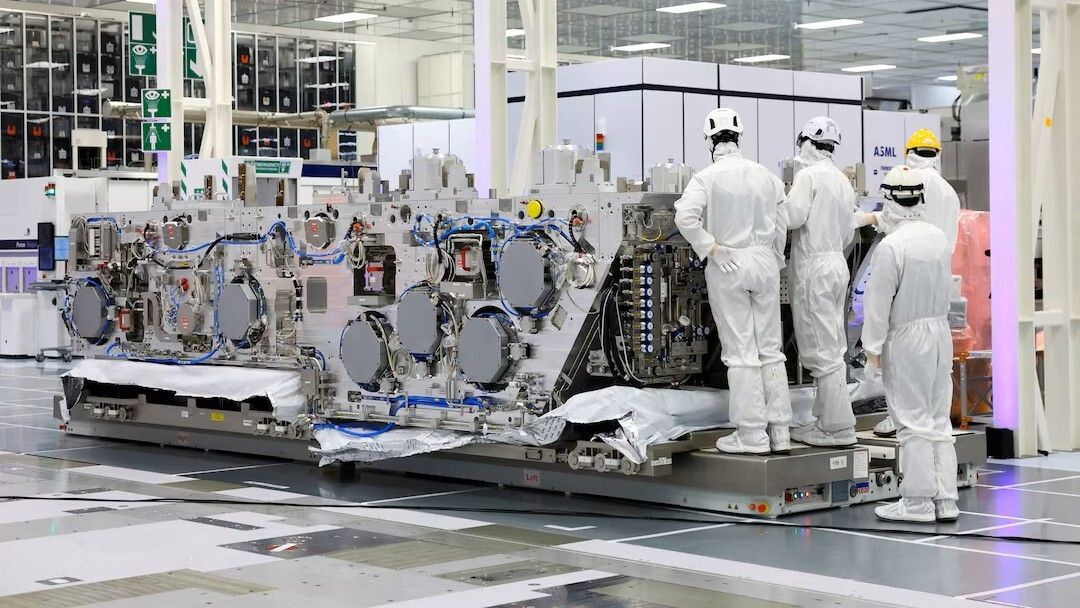
- Manufacturing Convergence: Imec has successfully fabricated the world's first quantum dot qubit device using High-Numerical Aperture (High-NA) Extreme Ultraviolet (EUV) lithography, proving quantum processors can utilize standard 300mm silicon semiconductor fabs.
- Timeline Compression: The breakthrough eliminates the traditional chasm between bespoke, cryogenic laboratory physics and mass-production CMOS manufacturing, potentially accelerating industrial-scale quantum computing timelines by up to a decade.
- Capital Allocation Shift: Enterprise tech giants and venture allocators are re-evaluating capital expenditure (CapEx) models, anticipating that next-generation AI accelerators and quantum co-processors will share unified infrastructure pipelines.
- Supply Chain Realignment: Legacy lithography bottlenecks dissolve as advanced foundry nodes (such as ASML’s Twinscan EXE systems) are repurposed to print sub-nanometer quantum dot arrays with unprecedented pitch precision.
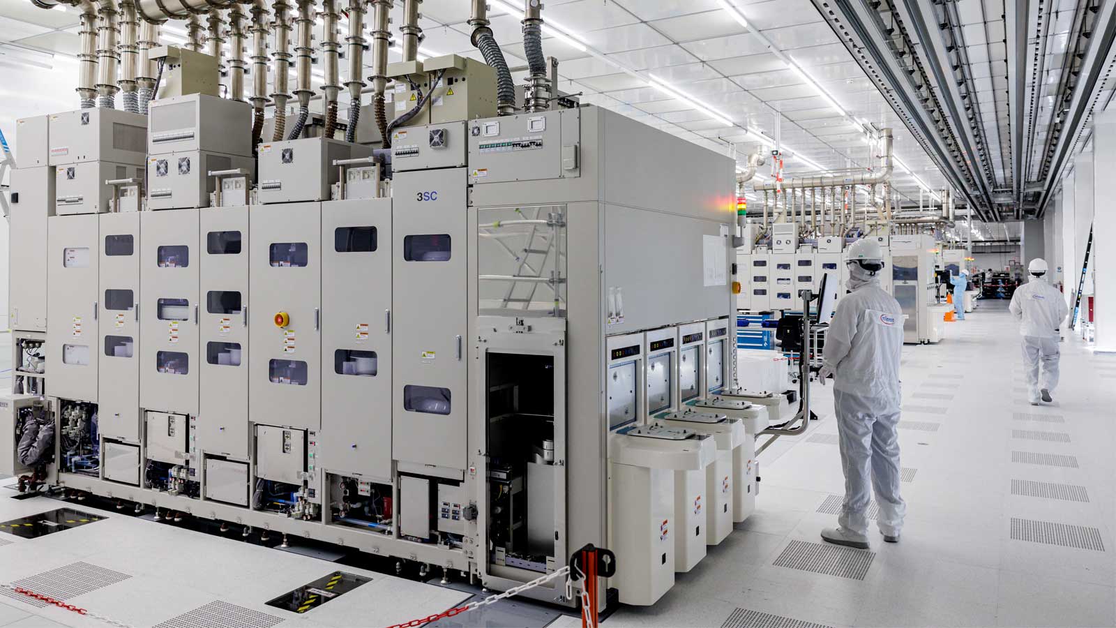
For three decades, the prevailing narrative surrounding quantum computing was one of architectural apartheid. While classical computing scaled exponentially atop the predictable, highly automated rails of Moore’s Law and complementary metal-oxide-semiconductor (CMOS) manufacturing, quantum computing remained trapped in the realm of artisanal physics. Building a qubit array required bespoke, ultra-cleanroom environments, manual wire-bonding, and fragile, non-standard material stacks that defied integration into high-volume wafer fabs. That narrative officially fractured in May 2026.
In a watershed development reported by Tom's Hardware, research and nanoelectronics hub Imec announced the successful fabrication of the world’s first quantum dot qubit device utilizing High-NA EUV lithography. By leveraging the industry's most advanced lithographic tooling—equipment typically reserved for sub-2nm artificial intelligence accelerators and high-performance computing (HPC) CPUs—Imec has done more than just build a better quantum chip. They have pulled the quantum computing paradigm onto the exact same industrial manufacturing roadmap as next-generation AI processors, fundamentally resetting enterprise risk assessment, valuation multiples, and infrastructure scalability models across the global technology sector.
The Physics of Convergence: Overcoming the Nanoscale Barrier
To understand the profound market liquidity and valuation implications of Imec’s breakthrough, one must examine the acute engineering impasse that has plagued spin-based and semiconductor quantum dots. Unlike superconducting circuits, which require massive physical footprints that complicate multi-million-qubit scaling, silicon spin qubits promise density. By trapping individual electrons inside gate-defined quantum dots within isotopically purified silicon, manufacturers can theoretically pack millions of qubits onto a standard postage-stamp-sized die.
However, theory collided violently with manufacturing reality. To isolate individual electrons and manipulate their spin states with atomic precision, gate electrodes must be patterned at sub-10nm critical dimensions with virtually zero line-edge roughness. Previous-generation standard EUV lithography (0.33 NA) strained under the weight of this requirement, necessitating multi-patterning techniques that introduced stochastic defects, dopant scattering, and thermal drift—fatal flaws for quantum coherence.
Imec’s deployment of High-NA EUV (0.55 NA) lithography bypasses these compounding manufacturing errors. With a single exposure, High-NA systems project finer feature sizes and sharper image contrasts onto the silicon wafer. By successfully applying this technology to quantum dot gate stacks, Imec achieved sub-nanometer overlay precision across a 300mm wafer. This technical feat proves that quantum dot architecture is no longer incompatible with standard 300mm fabrication lines. Instead, it can be slotted directly into existing foundry workflows.
Verified Data & Metrics Breakdown
| Metric / Parameter | Traditional Laboratory Approach | Imec High-NA EUV Breakthrough (2026) | Enterprise Impact & ROI Implication |
|---|---|---|---|
| Lithography Platform | Deep Ultraviolet (DUV) / E-Beam / 0.33 NA EUV with multi-patterning | 0.55 Numerical Aperture (High-NA) EUV (Single Exposure) | Eliminates multi-patterning defect propagation; boosts wafer yield. |
| Wafer Substrate Scale | Bespoke smaller wafers (100mm / 200mm experimental lines) | Standard industrial 300mm CMOS semiconductor wafers | Enables immediate fab integration and economies of scale. |
| Qubit Integration Roadmap | Isolated from mainstream fab; 10+ year speculative lag | Harmonized with sub-2nm AI accelerator node pipelines | Compresses commercialization timelines by an estimated 5 to 7 years. |
| Critical Dimension Precision | High variance, prone to gate-pitch distortion | Sub-nanometer overlay accuracy across dense dot arrays | Directly enhances quantum coherence times and gate fidelity. |
Capital Allocation, Risk Mitigation, and Market Liquidity
From a financial perspective, the integration of quantum fabrication into standard CMOS lines solves the industry's most prohibitive barrier to entry: capital expenditure amortization. Historically, venture capitalists and corporate treasuries viewed quantum computing investments as high-risk, black-hole expenditures. Constructing dedicated, single-purpose fabrication facilities for exotic quantum architectures required billions of dollars in sunk capital with zero depreciation crossover to classical revenue streams.
Imec’s breakthrough completely realigns this risk-mitigation calculus. Tier-1 foundries—such as TSMC, Intel Foundry, and Samsung—do not need to build out entirely novel infrastructure ecosystems to manufacture quantum co-processors. Instead, they can dynamically allocate existing High-NA EUV manufacturing lines to alternate between producing next-generation AI silicon and silicon spin-qubit wafers based on real-time enterprise demand and market liquidity.
For institutional investors and enterprise risk officers, this cross-compatibility dramatically compresses valuation multiples risk. Cloud compute architecture providers can now forecast a clear capital expenditure path toward hybrid AI-quantum data centers. By leveraging existing cleanroom footprints, lithography scanners (each valued upwards of $350 million), and automated wafer-handling robotics, the cost per functional qubit is projected to drop precipitously over the next 36 to 60 months.
Industry & Market Implications: Winners and Losers
Every major technological paradigm shift redistributes wealth, and Imec’s High-NA EUV quantum milestone is no exception. The strategic fallout will ripple across the global semiconductor and enterprise technology landscape:
- The Winners: Advanced Lithography & Foundry Giants. ASML, as the sole provider of High-NA EUV systems, solidifies its irreplaceable monopoly position. Meanwhile, tier-1 foundries equipped with High-NA tooling become the exclusive contract manufacturers for sovereign and enterprise-grade quantum processors, unlocking lucrative new high-margin revenue streams.
- The Winners: Silicon Spin-Qubit Startups. Pure-play quantum firms that aligned their architectures with CMOS-compatible silicon spin qubits (such as Diraq, Quantum Motion, and silicon-focused academic spinouts) suddenly possess an immense competitive advantage over superconducting and trapped-ion rivals tethered to bespoke manufacturing methods.
- The Losers: Bespoke Quantum Hardware Vendors. Companies that relied on proprietary, non-standard fabrication methodologies face an existential modernization crisis. Re-architecting established qubit designs to fit standard 300mm CMOS rules requires massive engineering pivots and exposes them to aggressive time-to-market pressure from fab-compatible competitors.
- The Losers: Legacy Cleanroom Equipment Makers. Niche, low-volume toolmakers catering exclusively to boutique academic labs and custom quantum fabrication lines will see their addressable total market contract as tier-1 foundries absorb volume production.
Frequently Asked Questions (People Also Ask)
What makes Imec’s use of High-NA EUV for quantum dots a breakthrough?
High-NA EUV (0.55 numerical aperture) provides superior optical resolution and single-exposure precision compared to older 0.33 NA lithography. Imec's application of this tool to silicon quantum dots proves that quantum gate arrays can be patterned with the exact sub-nanometer accuracy required for massive qubit density, eliminating the stochastic defects introduced by multi-patterning techniques.
How does this breakthrough impact the timeline for commercial quantum computing?
By demonstrating that quantum devices can be fabricated on standard 300mm silicon CMOS lines, Imec bridges the gap between laboratory research and high-volume manufacturing. Industry analysts estimate this harmonization could accelerate the timeline for commercial, fault-tolerant industrial quantum computers by up to a decade, bringing production horizons closer to the late 2020s and early 2030s.
Why are silicon spin qubits considered superior for mass manufacturing?
Silicon spin qubits utilize the existing manufacturing infrastructure, physics, and material science of the multi-trillion-dollar semiconductor industry. Because they are manufactured on standard silicon wafers using automated CMOS tools, they avoid the severe physical scaling limitations and custom packaging bottlenecks that handicap alternative architectures like superconducting circuits.
Will this integration affect enterprise cloud compute and AI data center infrastructure?
Yes. As quantum co-processors are pulled onto the same fabrication roadmap as advanced AI accelerators, enterprise architects can plan for heterogeneous compute nodes—where classical AI processors handle deterministic workloads and quantum co-processors tackle intractable optimization and molecular simulation tasks—within unified, liquid-cooled data center frameworks.
Future Outlook: The Road Ahead to 2030
As the industry digests the operational implications of Imec’s May 2026 announcement, the focus shifts immediately to execution milestones. The coming twenty-four months will witness a ferocious race to transition these single-device wafer proofs into multi-qubit logical processors operating with fault-tolerant error correction.
Key regulatory, supply chain, and engineering milestones to monitor include:
- Foundry Pilot Lines (H2 2026 - 2027): Watch for tier-1 foundry announcements regarding dedicated multi-project wafer (MPW) runs incorporating silicon spin-qubits alongside 2nm/1.4nm AI accelerator production.
- Cryogenic Packaging Scalability: Engineering breakthroughs in high-density, multi-layer high-frequency wiring capable of routing control signals from room-temperature CMOS control chips down to millikelvin quantum arrays on standard 300mm substrates.
- Error Correction Benchmarks: Validation of logical qubit fidelity manufactured via high-volume foundry tools versus historical artisanal lab benchmarks.
Imec has effectively closed the curtain on the era of artisanal quantum physics. By wedding the sub-nanometer precision of High-NA EUV lithography to the relentless scaling power of the global semiconductor foundry ecosystem, quantum computing has crossed the threshold from academic curiosity into hard corporate reality. For enterprise leadership, the mandate is clear: strategic capital allocation models, cloud architecture roadmaps, and AI infrastructure strategies must now account for a unified, silicon-based quantum future.