Executive Takeaways
Test Our Free AI & Tech Utilities Suite
Calculate LLM API token costs, analyze article dwell-time, or simulate tech DCA returns.
- Unprecedented Sovereign Backstopping: The Indian federal government's modified $10 billion India Semiconductor Mission (ISM) guarantees a flat 50% capital expenditure (capex) subsidy for fabs and packaging units, supplemented by state-level top-ups that reduce effective project capex by up to 70% to 75%.
- The Anchor Manufacturing Hubs: Commercial execution is moving rapidly from policy formulation to physical cleanrooms, anchored by Tata Electronics’ $11 billion foundry in Dholera (in partnership with Taiwan’s PSMC) and advanced packaging (ATMP/OSAT) mega-sites led by Micron Technology, CG Power-Renesas, and Kaynes Semicon.
- Strategic Focus on Trailing-Edge Nodes: Rather than entering the capital-destructive sub-3nm leading-edge race, India is strategically capturing mature, high-margin trailing-edge nodes (28nm to 90nm) that power automotive platforms, industrial automation, power electronics, and IoT devices.
- Infrastructure and Supply Chain Bottlenecks: Long-term economic viability hinges on resolving critical micro-utility dependencies, including continuous mega-watt clean energy grids, ultra-pure water (UPW) infrastructure, specialty gas supply chains, and transitioning domestic chip design talent from contract engineering services to proprietary IP ownership.
The Sovereign Push: De-risking Global Silicon Supply Chains

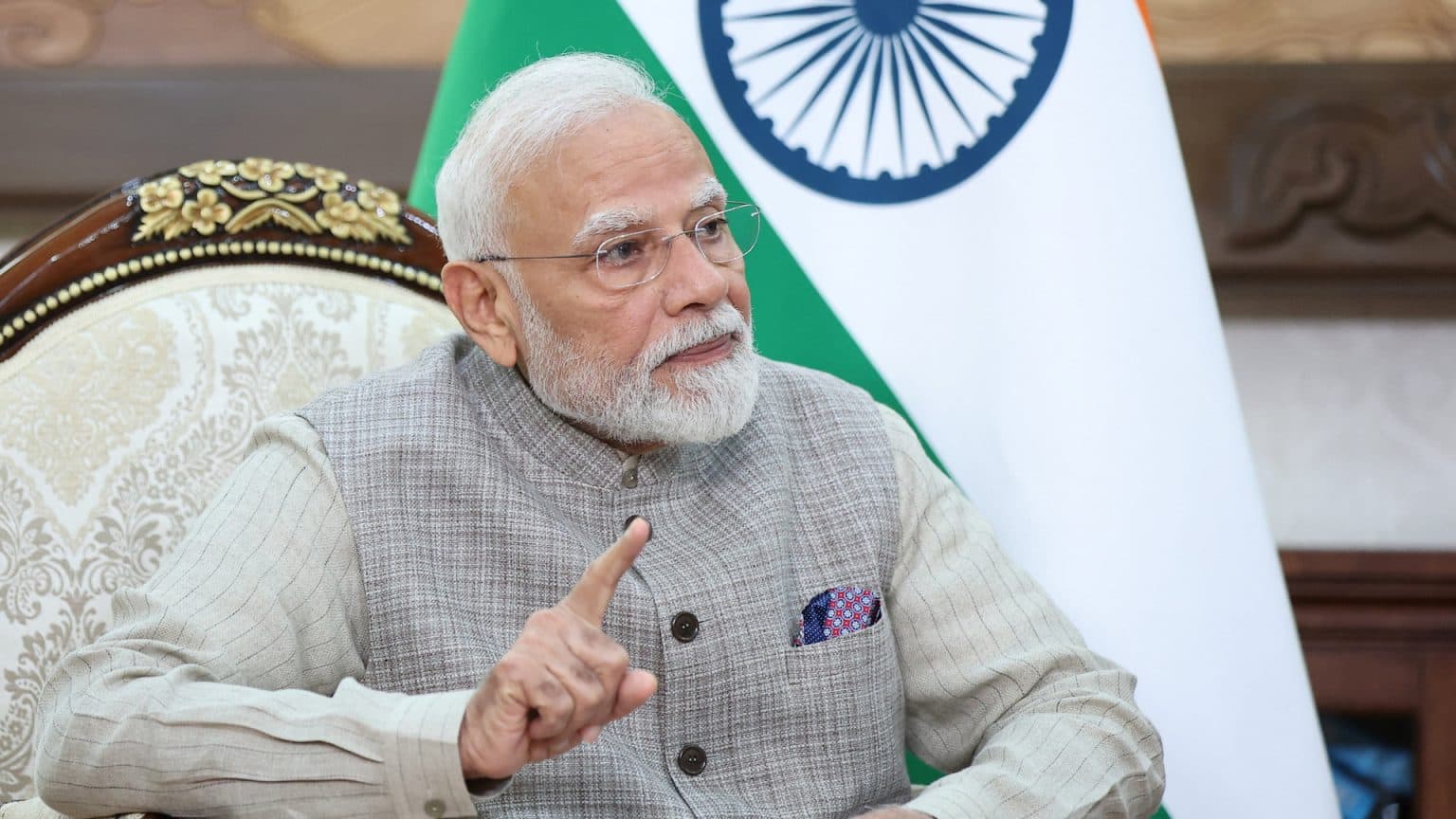
As multinational technology enterprises and defense conglomerates accelerate "China+1" diversification strategies, the Republic of India has mounted one of the most aggressive state-subsidized industrial pivots in modern economic history. Driven by post-pandemic semiconductor shortages that disrupted global automotive assembly lines and exposed vulnerable supply chains, New Delhi has repositioned silicon manufacturing as an urgent matter of national economic security and sovereign compute capability.
At the epicenter of this strategy sits the India Semiconductor Mission (ISM), backed by an initial $10 billion outlay under the Ministry of Electronics and Information Technology (MeitY). Unlike previous policy iterations that failed due to bureaucratic friction and capital allocation deficits, the revised framework offers a standardized, transparent incentive structure: a uniform 50% fiscal support mechanism on a par-value basis for silicon fab construction, display fabs, compound semiconductors, and Assembly, Testing, Marking, and Packaging (ATMP) or Outsourced Semiconductor Assembly and Test (OSAT) facilities.
When combined with state-level capital subsidies—most notably from industrial corridors in Gujarat, Maharashtra, and Tamil Nadu—international and domestic consortia are securing sovereign co-funding that covers between 65% and 75% of total project expenditures. This unprecedented de-risking strategy drastically alters the internal rate of return (IRR) calculations for multinational chipmakers, elevating India from an offsite R&D operational base into an emerging global hub for front-end fabrication and back-end chip integration.
The Industrial Map: Key Players, Mega-Fabs, and Strategic Alliances
India’s emergent semiconductor ecosystem is taking shape through a combination of domestic industrial titans, global outsourced foundries, and foreign technology transfer partnerships. The strategic intent is to build an interconnected value chain encompassing front-end wafer fabrication, mid-stream OSAT capabilities, and back-end system-level integration.
1. Tata Electronics & PSMC (Dholera, Gujarat)
The centerpiece of India’s front-end manufacturing ambition is the flagship commercial fab being erected by Tata Electronics in partnership with Taiwan’s Powerchip Semiconductor Manufacturing Corporation (PSMC) in Dholera, Gujarat. Representing a total capital outlay exceeding $11 billion (INR 91,000 crore), the facility is engineered for an initial monthly output capacity of 50,000 wafer starts per month (WPM).
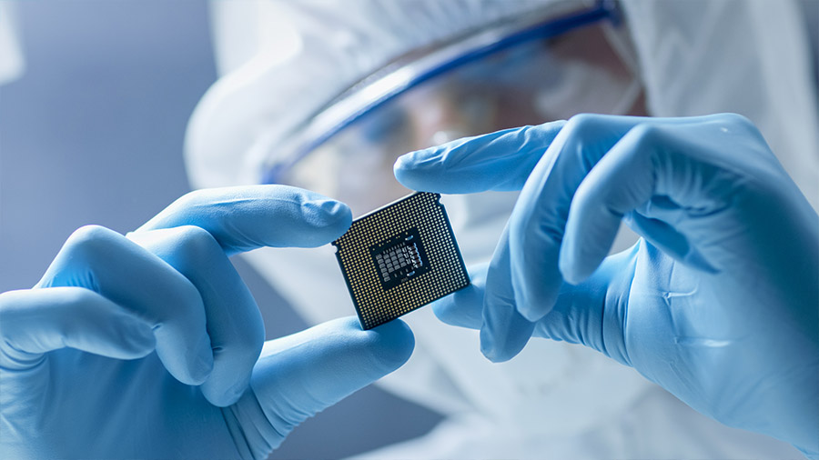
Crucially, the Dholera fab focuses on high-volume trailing-edge nodes, specifically 28nm, 40nm, 55nm, and 90nm manufacturing process technologies. These mature nodes do not require hyper-expensive Extreme Ultraviolet (EUV) lithography systems, yet they constitute the operational backbone for automotive microcontrollers, power management integrated circuits (PMICs), display driver ICs, and high-reliability industrial microprocessors. By capturing this volume, Tata and PSMC are positioning themselves as critical suppliers to domestic and global automotive Tier-1 suppliers and consumer device manufacturers.
2. Micron Technology (Sanand, Gujarat)
Serving as the operational wedge for back-end semiconductor manufacturing, Micron Technology’s $2.75 billion memory assembly and test facility in Sanand, Gujarat, represents one of the largest single foreign direct investments in India's tech hardware domain. Backed by $1.37 billion in combined central and state incentives, the plant transforms raw DRAM and NAND flash wafers imported from Micron's global fabs into integrated memory modules, enterprise solid-state drives (SSDs), and high-density packaging solution matrices for mobile and cloud data center markets.
3. CG Power, Renesas, and Stars Microelectronics (Sanand, Gujarat)
A joint venture uniting India’s Tube Investments subsidiary CG Power with Japan’s Renesas Electronics Corporation and Thailand’s Stars Microelectronics is constructing a $900 million OSAT unit in Sanand. Renesas provides crucial proprietary microcontroller and analog chip architecture expertise, allowing the joint venture to produce specialized chips tailored to space technology, electric vehicles (EVs), renewable energy inverters, and smart grid automation hardware.
4. Kaynes Semicon and Emerging Regional Players
Underscoring the rapid expansion of domestic electronics manufacturing services (EMS) into advanced packaging, Kaynes Semicon (a subsidiary of Kaynes Technology) is deploying over $330 million to build an OSAT plant in Sanand, Gujarat. Featuring automated cleanrooms and advanced multi-chip module (MCM) capabilities, Kaynes is targeting high-density interconnect applications for industrial automation, smart energy meters, and aerospace defense systems.
Verified Capital Allocation & Project Specifications
The table below provides a detailed structural breakdown of major semiconductor manufacturing and packaging projects approved and progressing across India's domestic ecosystem:
| Consortium / Enterprise | Foreign Tech Partner | Primary Capability / Facility Type | Facility Location | Estimated Capex (USD) | Node Architecture / Target Verticals |
|---|---|---|---|---|---|
| Tata Electronics | PSMC (Taiwan) | Front-End Commercial Wafer Fab | Dholera, Gujarat | $11.0 Billion | 28nm, 40nm, 55nm, 90nm (Automotive, PMIC, Industrial) |
| Micron Technology | Proprietary (USA) | Advanced ATMP / OSAT (Memory) | Sanand, Gujarat | $2.75 Billion | DRAM & NAND Flash Module Packaging (Cloud, Mobile) |
| CG Power JV | Renesas (Japan) & Stars Micro (Thailand) | OSAT / Specialty Chip Packaging | Sanand, Gujarat | $900 Million | Analog, Microcontrollers, Smart Power (EVs, Industrial) |
| Kaynes Semicon | Technology Transfer Partners | OSAT / Multi-Chip Modules | Sanand, Gujarat | $330 Million | Industrial Automation, Smart Meters, Avionics |
| Tower / Adani (Proposed) | Tower Semiconductor (Israel) | Analog & Compound Wafer Fab | Panvel, Maharashtra | $10.0 Billion | 65nm/180nm Analog, RF, SiGe, Power Semiconductors |
The Design Advantage: Upgrading the Value Chain
While physical fab construction commands broad publicity, India's most mature competitive moat resides in fabless semiconductor design. The country currently houses over 20% of the world’s chip design workforce. Global technology leaders—including Qualcomm, Nvidia, Intel, Texas Instruments, Broadcom, and MediaTek—operate vast R&D engineering operations across Bengaluru, Hyderabad, Noida, and Pune.
Historically, these engineering centers served as back-office execution assets for parent corporations headquartered in Silicon Valley or Hsinchu. However, New Delhi's Design Linked Incentive (DLI) scheme—a financial support program offering financial offsets for EDA (Electronic Design Automation) software tool deployment, tape-out expenses, and IP core acquisition—is fundamentally altering this operational dynamic.
Domestic startups and established chip design operations are moving up the margin curve, acquiring native intellectual property (IP) and engineering original chip architectures tailored to RISC-V open-source platforms, edge-AI acceleration, biometric processing, and localized power management systems. This design ecosystem ensures that incoming domestic foundries will benefit from built-in local tape-out demand, establishing a self-sustaining domestic cycle from initial chip layout to physical fabrication and testing.
Structural Execution Risks: Infrastructure, Chemicals, and Yields
Despite significant sovereign backing, transforming greenfield sites into high-yield semiconductor fabrication complexes entails substantial operational risks. Semiconductor manufacturing ranks among the most precision-intensive industrial activities on Earth, where minor micro-environmental fluctuations can destroy entire production runs.
- Ultra-Pure Water (UPW) Systems: A modern commercial wafer fab processing 50,000 WPM consumes millions of gallons of water daily. Fabs require Ultra-Pure Water filtered down to sub-ppb (parts-per-billion) impurity thresholds. Establishing reliable, closed-loop UPW treatment infrastructure in arid industrial zones like Dholera demands uninterrupted industrial engineering execution.
- Grid Reliability & Power Quality: Fab production lines cannot tolerate voltage sags lasting mere milliseconds. Micro-disruptions cause stepper misalignment and catastrophic wafer loss. Ensuring ultra-stable, grid-scale power delivery backed by redundant sub-stations and localized battery energy storage systems (BESS) remains an absolute operational prerequisite.
- Specialty Chemical & Gas Supply Chains: Front-end fabrication relies on a highly specialized network of high-purity gases (silane, phosphine, arsine) and electronic-grade wet chemicals (hydrofluoric acid, high-purity hydrogen peroxide). India remains heavily dependent on foreign imports for these ultra-high-purity raw inputs, leaving initial fab operations exposed to external maritime supply chain shocks.
- Talent Upskilling for Cleanroom Operations: While India possesses an abundance of high-level chip design engineers, it faces a deficit of operational technicians, cleanroom managers, process yield engineers, and photolithography specialists. Overcoming this talent gap requires structured, cross-border training initiatives with Taiwanese, Japanese, and European technical institutes.
Industry & Market Implications
The institutional execution of India’s semiconductor policy carries profound economic implications across local, regional, and global trade corridors:
Winners
- Global Automotive and Industrial OEMs: Domestic manufacturing of 28nm-90nm microcontrollers and power management ICs provides Tier-1 suppliers with an alternative sourcing hub, mitigating concentration risk in East Asia.
- Domestic EMS and Hardware Startups: Local assembly houses and consumer electronics manufacturers will see reduced component procurement lead times, accelerating time-to-market and elevating localized value addition from 15% toward global benchmarks above 40%.
- Enterprise Engineering Services: Indian technology consulting firms and localized engineering service operators will capture lucrative high-eCPM contracts spanning fab construction management, facility software integration, and yield optimization modeling.
Challenges & Realities
- Southeast Asian Packaging Hubs: Incumbent packaging and testing hubs in Malaysia, Vietnam, and the Philippines face long-term regional competition as India aggressively captures greenfield ATMP expansion capital.
- Capital Depreciation Pressure: Fabs demand continuous capital reinvestment to replace legacy equipment and upgrade lithography systems. If yield rates lag international standards during initial ramp phases, state and private partners face extended timeframes to achieve enterprise profitability.
Frequently Asked Questions (People Also Ask)
Why is India prioritizing trailing-edge mature nodes over leading-edge sub-3nm processes?
Developing sub-3nm leading-edge capability requires dozens of billions of dollars per facility, access to advanced EUV (Extreme Ultraviolet) lithography technology from ASML, and decades of yield optimization expertise. Mature nodes (28nm to 90nm) represent over 60% of total global semiconductor volume demand, powering critical automotive, industrial, defense, and power management applications. Focusing on mature nodes minimizes capital risk, matches existing localized industrial demand, and delivers a faster path to commercial viability and sustainable factory utilization rates.
What structural financial incentives are available to semiconductor investors in India?
Under the India Semiconductor Mission (ISM), the central government offers a uniform 50% capital subsidy on a par-value basis for the setting up of silicon fabs, compound semiconductor plants, display foundries, and ATMP/OSAT packaging facilities. Additionally, individual state governments provide complementary fiscal incentives—including state capex top-ups (typically 10% to 25%), subsidized land acquisition, long-term power tariff concessions, stamp duty exemptions, and infrastructure support for water and connectivity.
How does India's existing design talent support its semiconductor ambitions?
India hosts approximately 20% of the world’s global chip design talent pool, working within localized R&D branches of global semiconductor majors. Through the Design Linked Incentive (DLI) scheme, India is capitalizing on this foundation by subsidizing domestic fabless design startups, providing access to expensive Electronic Design Automation (EDA) tools, and offsetting initial tape-out costs. This domestic design capability creates a direct local customer pipeline for native foundries and packaging plants.
What are the biggest operational risks to sustaining fab operations in India?
The primary operational risks include securing continuous 99.9999% uptime electrical power, developing localized high-purity chemical and specialty gas supply chains, maintaining massive ultra-pure water (UPW) capacity, and upskilling technicians for high-yield cleanroom operations. Mitigating these risks requires seamless coordination between central infrastructure authorities, state utility providers, and specialized international vendor ecosystems.
Future Outlook: The Road to 2030
Over the next five to seven years, India’s semiconductor evolution will transition from foundational construction into operational ramp-up and yield-curve optimization. As the initial facilities constructed by Tata Electronics, Micron, and CG Power achieve commercial volume production, foreign equipment vendors, chemical purifiers, and substrate suppliers will establish localized support operations around primary clusters in Gujarat, Maharashtra, and Southern India.
The strategic objective for 2030 extends beyond trailing-edge silicon. Over time, India aims to leverage its foundation in mature nodes to advance into high-margin niche markets, including compound semiconductors (Silicon Carbide and Gallium Nitride for EV power electronics), advanced heterogenous integration (3D packaging and chiplets), and specialized RF (radio frequency) modules for global 6G telecommunications. With sovereign fiscal backing, global geopolitical tailwinds, and an unmatched engineering talent reserve, India is executing a structural transformation designed to permanently carve out a resilient, high-value node in the global semiconductor footprint.