Executive Takeaways
- Unprecedented Density: IBM Research successfully prototyped the world's first 2-nanometer (nm) gate-all-around (GAA) nanosheet test chip, packing an astonishing 50 billion transistors onto a fingernail-sized piece of silicon.
- Macroeconomic & Capital Impact: The breakthrough arrives at a critical juncture of global supply chain strain, shifting geopolitical capital allocation, and soaring enterprise demand for hyper-efficient cloud compute architecture.
- Performance Multipliers: Compared to prevailing 7nm commercial nodes, the 2nm architecture targets a 45% performance boost or a 75% reduction in power consumption, fundamentally rewriting enterprise ROI equations for data centers.
- Strategic Inflection: While immediate mass production remains on a multi-year horizon, this engineering milestone reshapes valuation multiples, intellectual property leverage, and risk mitigation strategies across the global semiconductor ecosystem.
NEW YORK — In the high-stakes theater of advanced semiconductor manufacturing, incremental progress is often celebrated as revolution. But when IBM Research unveiled the world’s first 2-nanometer (nm) test chip featuring 50 billion transistors on May 6, 2021, the announcement transcended typical industry PR. It signaled a profound structural shift in the physics of computing—one with cascading implications for enterprise technology portfolios, global market liquidity, and the geopolitical balance of technological supremacy.
For decades, Moore’s Law—the empirical observation that the number of transistors on a microchip doubles roughly every two years—has governed the rhythm of the global economy. Yet, as lithography approached single-digit nanometer thresholds, quantum tunneling, thermal dissipation, and severe manufacturing bottlenecks threatened to halt progress entirely. IBM’s breakthrough at the Albany NanoTech Complex in New York did not merely kick the horizon further down the road; it fundamentally redefined what is physically possible inside a silicon wafer.
The Architectural Genesis: How IBM Overcame the Nanosheet Barrier
Test Our Free AI & Tech Utilities Suite
Calculate LLM API token costs, analyze article dwell-time, or simulate tech DCA returns.
To understand the profound nature of IBM's 2nm milestone, one must examine the engineering dead-end that preceding architectures were rapidly approaching. For years, FinFET (Fin Field-Effect Transistor) technology served as the industry workhorse, scaling down from 16nm to 7nm and even probing 5nm designs. However, as gate lengths shrink below the 5nm threshold, the control of current leakage via standard fin structures degrades significantly.
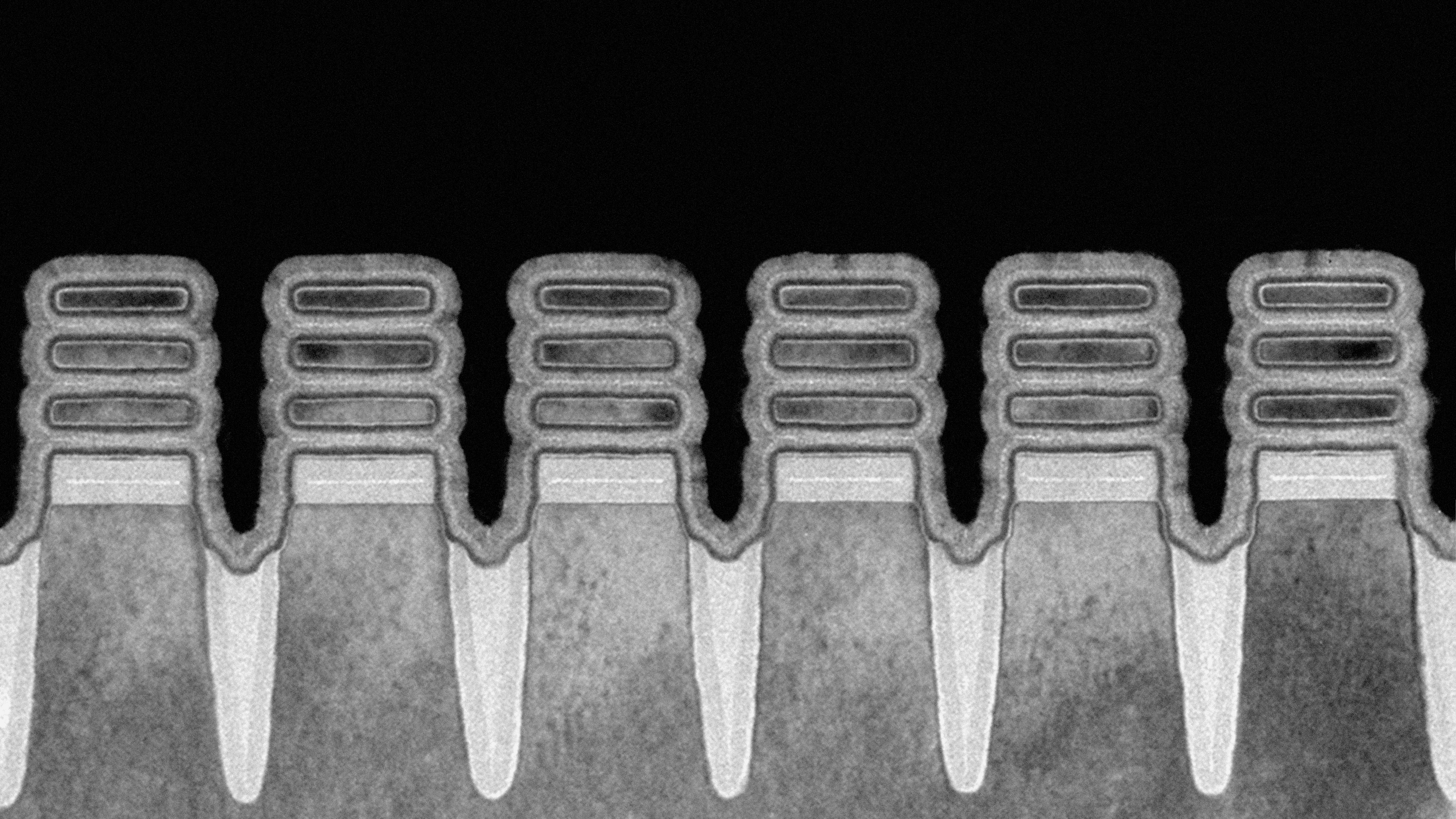
IBM’s research team bypassed this physical limitation by pioneering a vertical stack of silicon nanosheets. In this gate-all-around (GAA) architecture, the gate material wraps completely around each nanosheet channel, maximizing electrostatic control and virtually eliminating current leakage when the transistor is in an "off" state. This precision engineering enabled researchers to pack 50 billion transistors onto a die measuring a mere 150 square millimeters.
"The IBM chip announced today reflects the ingenuity of IBM and its continuous commitment to hard physics innovation," said Darío Gil, Senior Vice President and Director of IBM Research at the time of the announcement. By allowing the physical width of each nanosheet to be adjusted during manufacturing, IBM unlocked a level of circuit design flexibility previously unattainable in sub-3nm nodes.
Financial, Operational, and Infrastructure Implications
For chief information officers, corporate treasurers, and institutional investors, hardware density is no longer merely an engineering metric; it is a primary driver of enterprise ROI and operating margin sustainability. The operational economics of modern hyperscale data centers are fundamentally constrained by power consumption and thermal management.
Consider the core value propositions unlocked by a 2nm transition:
- Power Efficiency: Achieving a 75% reduction in power consumption relative to 7nm nodes allows cloud providers to scale compute capacity exponentially without triggering localized grid instability or prohibitive cooling expenditures.
- Compute Velocity: A 45% performance increase at the same power envelope dramatically compresses processing times for complex workloads, including financial risk modeling, real-time algorithmic trading, and large-scale cryptographic encryption.
- Mobile and Edge Infrastructure: For mobile device ecosystems, a quadrupling of battery life transforms edge computing capabilities, enabling sophisticated on-device artificial intelligence inference without reliance on latency-prone cloud round-trips.
From a capital allocation perspective, this technological leap validates heavy ongoing investments in advanced research and development. Semiconductor capital expenditure cycles are notoriously capital-intensive, requiring billions in upfront outlays before realizing commercial payback. IBM’s successful prototyping de-risks the early-stage physics for its foundry partners—most notably Samsung and Intel—paving the way for structured technology-sharing agreements and licensing revenue streams that bolster long-term equity valuations.
Verified Data and Metrics Breakdown
To quantify the generational leap represented by IBM’s 2nm test chip, industry analysts benchmark the architecture against current and legacy production nodes:
| Node Generation | Transistor Density (approx.) | Primary Transistor Architecture | Key Performance / Power Trade-off |
|---|---|---|---|
| 7nm Commercial | ~90 to 100 million transistors / mm² | FinFET | Baseline standard for high-performance computing (2018–2020). |
| 5nm Commercial | ~130 to 170 million transistors / mm² | Advanced FinFET | Incremental 15% speed increase or 30% power reduction over 7nm. |
| IBM 2nm Prototyped | ~333 million transistors / mm² (50B on 150mm²) | Gate-All-Around (GAA) Nanosheet | +45% performance or -75% power consumption compared to 7nm. |
Frequently Asked Questions (People Also Ask)
What makes IBM's 2nm test chip significantly different from previous nodes?
Unlike traditional FinFET architectures that utilize vertical fins to control electrical current, IBM's 2nm design relies on gate-all-around (GAA) nanosheets. This vertically stacked structure wraps the gate material entirely around the channel, drastically reducing current leakage and enabling an unprecedented density of 50 billion transistors on a chip the size of a fingernail.
When will 2nm semiconductors become commercially available for enterprise and consumer markets?
While IBM successfully demonstrated working prototypes, commercial high-volume manufacturing (HVM) requires extensive tooling adjustments, supply chain synchronization, and yield optimization. Industry projections generally point toward initial commercial volume production entering the market several years post-prototype debut, as foundries adapt their extreme ultraviolet (EUV) lithography lines to accommodate nanosheet fabrication.
How does the 2nm architecture impact data center energy consumption and enterprise IT costs?
Data centers face severe operational constraints regarding power availability and thermal dissipation. By offering up to a 75% reduction in power consumption for equivalent workloads—or delivering a 45% performance boost—2nm technology directly mitigates escalating utility overhead, lowers cooling expenditures, and extends the operational lifespan of enterprise server infrastructure.
Who manufactures IBM’s chips, and how does this impact the global semiconductor supply chain?
IBM primarily operates as a research and systems powerhouse, often partnering with major global foundries—such as Samsung and Intel—to transfer its foundational IP into commercial manufacturing pipelines. This collaborative model acts as a vital technological catalyst, diversifying intellectual property away from single-source geopolitical choke points and reinforcing resilient supply chain frameworks.
Future Outlook: Navigating the Road to Commercialization
As the semiconductor industry digests the long-term ramifications of IBM’s breakthrough, attention inevitably turns toward execution risk and manufacturing scale. Prototyping a test chip in a controlled research environment is a monumental achievement; however, scaling yields to commercially viable levels across millions of wafers is the ultimate test of industrial engineering.
Key milestones to monitor over the upcoming quarters include:
- Foundry Integration: The successful transfer of GAA nanosheet process technology into commercial fabrication plants (fabs) operated by IBM alliance partners.
- EUV Tooling Advancements: Further refinements in High-Numerical Aperture (High-NA) Extreme Ultraviolet lithography equipment necessary to pattern sub-2nm features with atomic precision.
Ecosystem Adoption: Early enterprise design wins and proof-of-concept server architectures optimized specifically for the thermal and electrical profiles of nanosheet silicon.
Ultimately, IBM’s 2nm milestone serves as definitive proof that reports of the death of Moore’s Law have been greatly exaggerated. While the capital intensity and engineering hurdles required to push silicon physics forward are higher than ever, the rewards—spanning enhanced national security, resilient supply chains, and unprecedented enterprise compute efficiency—ensure that the race for the atomic frontier will continue to accelerate unabated.