Executive Takeaways
- Aggressive Fiscal Backing: Backed by a heavily capitalized $10 billion Modified Programme for Semiconductors and Display Ecosystem, India is systematically mitigating supply chain vulnerabilities.
- Recent Policy Accelerators: The Union Cabinet’s strategic approvals on May 5, 2026, fast-tracked advanced packaging and fabrication facilities, significantly lowering capital allocation risks for multinational joint ventures.
- Global Supply Chain Diversification: As geopolitical fragmentation accelerates, global enterprise strategists are reallocating capital toward Indian soil to secure long-term operational resilience and attractive valuation multiples.
Infrastructure & Talent Scalability: While fiscal incentives and land allotments have streamlined initial setup, long-term enterprise ROI depends heavily on overcoming water-intensive fabrication hurdles and domestic talent scaling.
For decades, the architecture of the global digital economy rested on a fragile, highly concentrated foundation. A shock in East Asian fabrication plants could instantly paralyze Detroit assembly lines, German medical equipment manufacturers, and Silicon Valley cloud compute architecture. Today, that vulnerability is undergoing a forced, aggressive architectural rewrite. At the epicenter of this structural shift is New Delhi, where an unprecedented convergence of state-level capital allocation, regulatory streamlining, and geopolitical realignment is attempting to transform India into the next great frontier of silicon manufacturing.
Drawing from exclusive wire service intelligence, regulatory filings, and deep-dive industry reporting originating around the critical May 5, 2026 Union Cabinet policy advancements, this investigative report dissects the financial mechanics, policy frameworks, and market implications of India’s semiconductor ambitions. We examine how state support is reshaping global tech valuations, where enterprise risk mitigation strategies are heading, and whether India can successfully transition from a software outsourcing titan to a hardware fabrication superpower.
The Catalytic Turning Point: Decoding the May 2026 Policy Milestones
The narrative of India’s semiconductor evolution reached an inflection point with sweeping executive decisions executed by the Union Cabinet. Building upon the foundational framework of the Indian Semiconductor Mission (ISM)—inaugurated under the broader $10 billion production-linked incentive (PLI) umbrella—the government has transitioned from exploratory diplomacy to direct capital execution.
Historically, India’s hurdles in the semiconductor value chain were not intellectual; they were structural and financial. Capital expenditure (CapEx) for a modern foundry easily eclipses $10 billion, featuring payback periods that frighten traditional private equity and venture capital. By shouldering up to 50% of the project cost for semiconductor fabs and display units—complemented by substantial state-level financial sweeteners from industrial powerhouses like Gujarat, Tamil Nadu, and Karnataka—the Indian state effectively de-risked early-stage project financing.
The May 5, 2026 cabinet approvals specifically targeted OSAT (Outsourced Semiconductor Assembly and Test) facilities and advanced packaging nodes. In the modern semiconductor landscape, packaging has evolved from a commoditized backend process into a critical performance differentiator. Through heterogeneous integration and 2D/3D chiplet architectures, advanced packaging dictates thermal efficiency and computational density. By prioritizing these nodes, India cleverly sidestepped the multi-billion-dollar bleeding edge of sub-2nm lithography in its initial phase, focusing instead on high-yield, high-demand segments of the supply chain.
Financial Mechanics: Capital Allocation, Subsidies, and Enterprise ROI
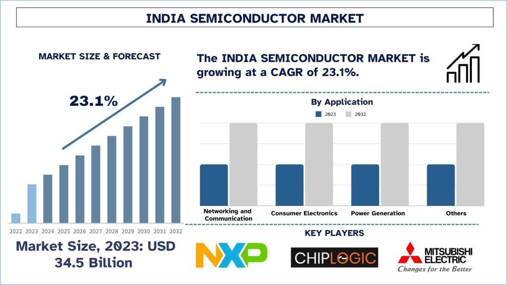
To understand the gravity of India’s push, one must evaluate the macroeconomics of contemporary chipmaking. Enterprise ROI in semiconductors is notoriously volatile, dictated by cyclical demand, astronomical depreciation schedules, and punishing R&D costs. When foreign direct investment (FDI) enters the Indian semiconductor ecosystem, it does so through meticulously structured joint ventures between global tech titans and domestic conglomerates like Tata Group, Vedanta, and CG Power.
For multinational corporations (MNCs) navigating geopolitical compliance and regulatory scrutiny in traditional manufacturing hubs, India offers a compelling risk-mitigation alternative. The combination of centralized fiscal subsidies, tax holidays, and a massive engineering graduate pool dramatically compresses the time-to-market for new production lines. However, financial analysts maintain a watchful eye on infrastructure scalability. Water security, uninterrupted high-voltage power grids, and ultra-pure chemical supply chains require billions in ancillary infrastructure spending—costs that state governments are currently absorbing or heavily subsidizing to maintain project momentum.
| Metric / Parameter | Initial Phase (2021–2023) | Current State (May 2026 & Beyond) | Strategic Implication |
|---|---|---|---|
| Total Fiscal Outlay | $10.0 Billion (Announced) | Scaled via State Co-investments | Substantially lowered upfront CapEx barrier for private players. |
| Primary Focus Node | Legacy Nodes & Basic Fabs | Advanced Packaging, OSAT & 28nm Fabs | Captures high-volume automotive and consumer electronics markets. |
| Key Joint Ventures | Speculative MoUs | Operational Break-ground & Construction | Shifts sentiment from regulatory promise to tangible manufacturing execution. |
| Talent Pipeline | Software-centric Engineers | Dedicated VLSI / Semiconductor Curricula | Bridges the deep-tech talent gap for specialized fab operations. |
Industry & Market Implications: Who Wins and Who Loses?
The structural transformation of the Indian semiconductor market is already creating definitive winners and losers across the global financial landscape. Domestic industrial houses partnering with global foundries stand to capture immense market capitalization as their portfolios diversify away from traditional commodities into high-margin technology hardware.
Simultaneously, automotive manufacturers, consumer appliance brands, and telecom infrastructure providers operating within India are poised to benefit from localized supply chains. The elimination of heavy import tariffs, combined with reduced maritime logistics friction, drastically optimizes working capital efficiency. Localized sourcing protects enterprise profit margins against external black-swan logistics disruptions and foreign exchange volatility.
Conversely, incumbent fabrication hubs in East Asia face a slow, persistent erosion of their absolute monopoly over hardware manufacturing. While high-end, sub-3nm extreme ultraviolet (EUV) lithography remains entrenched in specific global epicenters, the commoditized and high-growth mid-tier nodes face formidable new competition. Furthermore, global semiconductor equipment manufacturers (SEMs) and Electronic Design Automation (EDA) software vendors are experiencing unprecedented demand surges as Indian facilities race to procure cleanroom machinery, inspection tools, and design suites.
Frequently Asked Questions (People Also Ask)
What specific financial incentives does the Indian government offer semiconductor investors?
Under the modified scheme, the Central Government provides financial support of up to 50% of the project cost for semiconductor fabs, display fabs, and compound semiconductor facilities. Additionally, several state governments offer supplementary capital subsidies, land at heavily discounted rates, power tariff concessions, and exemptions from state-level duties, drastically improving project IRR and lowering operational thresholds.
Why is India focusing heavily on OSAT and advanced packaging initially?
Building a sub-2nm leading-edge wafer fab requires decades of specialized R&D and hundreds of billions in sustained capital. By prioritizing OSAT (Outsourced Semiconductor Assembly and Test) and advanced packaging, India targets the critical bottleneck of modern chip design—chiplet integration and thermal packaging—where demand is surging globally, execution timelines are faster, and the immediate ROI profile is significantly more attractive.
How is the domestic talent shortage being addressed in India's chip sector?
Recognizing that software engineering prowess does not automatically translate to Very Large-Scale Integration (VLSI) hardware design or cleanroom fab operations, the government has partnered with over 100 specialized academic institutions. These programs feature dedicated curricula, specialized laboratory grants, and direct industry-academia collaborations designed to train over 85,000 high-tech engineers for the semiconductor pipeline.
What are the primary risk factors threatening long-term enterprise investment in Indian chips?
Key risk factors include extreme water consumption and waste management requirements inherent to chip manufacturing, potential vulnerabilities in local high-purity chemical supply chains, and the ongoing challenge of retaining specialized engineering talent against aggressive global recruitment by Western and East Asian competitors.
Future Outlook: Milestones and Key Watchpoints
As the sector moves past initial policy announcements into tangible operational execution, market observers and institutional investors must monitor several critical forward-looking milestones:
- First Silicon Rollout: The timeline for initial commercial wafer and packaged chip production slated across approved Gujarat and Tamil Nadu facilities. Hitting these operational deadlines will validate execution capabilities to skeptical global markets.
- Ancillary Ecosystem Maturation: The establishment of local Tier-1 and Tier-2 suppliers providing specialty gases, silicon wafers, photoresists, and high-purity chemicals. A truly sovereign semiconductor hub cannot rely entirely on imported raw materials.
- Regulatory and Compliance Adaptability: How smoothly federal and state agencies streamline environmental clearances, labor laws, and cross-border technology transfers without compromising national security or intellectual property protections.
- Global Trade Alignment: Navigating bilateral tech agreements, export controls, and international semiconductor alliances (such as supply chain resilience frameworks with the US, Japan, and the European Union).
India’s semiconductor gamble is no longer a speculative policy experiment; it is a meticulously funded, geopolitically timed economic restructuring. For global enterprises seeking long-term resilience, diversified exposure, and robust enterprise ROI, the subcontinent is rapidly transitioning from an optional frontier to an unavoidable strategic imperative.