Executive Takeaways
- A Half-Century of Mastery: Dr. Kinam Kim’s career spans the exact arc of modern semiconductor evolution, tracing Samsung’s trajectory from an aggressive memory copycat to an undisputed architect of global compute infrastructure.
- From pioneering 3D FinFET architectures to scaling vertical NAND (V-NAND) flash memory, Kim’s engineering discipline fundamentally reshaped capital expenditure, enterprise ROI, and manufacturing scalability across the entire tech ecosystem.
- The strategic interplay between macroeconomic capital allocation, geopolitical supply-chain volatility, and relentless R&D reinvestment defined Kim’s tenure, offering a masterclass in long-term risk mitigation and valuation multiple expansion.
- As the industry enters the post-Moore’s Law era, Kim’s legacy serves as the strategic blueprint for next-generation advanced packaging, foundry dominance, and heterogeneous integration.
In the high-stakes theater of global semiconductor manufacturing, where billion-dollar capital expenditure cycles dictate the fortunes of nations and enterprise giants alike, few figures have cast a longer shadow than Dr. Kinam Kim. Over a career spanning nearly five decades, Kim did not merely witness the digital revolution—he engineered its foundational hardware. From his early days navigating the precarious physics of sub-micron scaling to his ascension as the Vice Chairman and CEO of Samsung Electronics’ Device Solutions division, Kim’s journey mirrors the miraculous, volatile, and profoundly influential rise of South Korea’s semiconductor empire.
For institutional investors, enterprise tech strategists, and global policymakers, understanding Kinam Kim’s blueprint is essential. At a time when semiconductor supply chains are weaponized as geopolitical leverage and valuation multiples hinge on micro-architectural breakthroughs, Kim’s career provides a masterclass in technological foresight, disciplined capital allocation, and relentless operational execution.
The Genesis of an Industrial Titan: Breaking Ground in Memory
When Kinam Kim entered the semiconductor ecosystem, the global memory market was dominated by entrenched American and Japanese conglomerates. Samsung, then a diversified industrial conglomerate helmed by visionary founder Lee Byung-chul, was viewed by Western incumbents as an aggressive upstart unlikely to master the hyper-complex physics of dynamic random-access memory (DRAM).
Kim, armed with a Ph.D. in Electrical Engineering from the University of California, Los Angeles (UCLA), joined Samsung during a critical juncture in the early 1980s. This was the era of the "Giga-project" mindset—a high-risk, counter-cyclical investment strategy where Samsung poured billions into R&D and fab construction precisely when global competitors were cutting budgets during market downturns. Kim’s technical acumen quickly singled him out as a rare hybrid: a brilliant device physicist who understood how to translate theoretical nanometer-scale mechanics into high-yield, mass-market manufacturing.
Under his technical leadership, Samsung relentlessly attacked the scaling limits of planar DRAM and NAND flash. When conventional wisdom dictated that physical barriers would halt miniaturization, Kim and his research teams pioneered radical material science innovations, shifting industry paradigms from aluminum interconnects to copper, and eventually mastering high-k metal gate technologies. These engineering feats did not just yield faster chips; they fundamentally compressed enterprise IT infrastructure costs, enabling the cloud computing revolution by driving down the cost-per-gigabit of storage.
Architecting the Third Dimension: The V-NAND and FinFET Revolutions
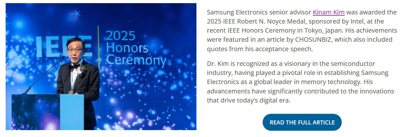
Perhaps Kim’s most consequential technical contribution was steering Samsung through the existential crisis of 2D NAND scaling limits. By the late 2000s, shrinking planar flash cells laterally had hit a brick wall of quantum tunneling interference and manufacturing uneconomic yields. The market consensus was that NAND flash had reached its physical terminal velocity.
Kim rejected this premise. Championing a radical architectural pivot, he spearheaded the commercialization of 3D NAND flash—commercially branded as V-NAND. Instead of packing cells closer together on a flat plane, Kim’s engineering teams stacked memory cells vertically like skyscrapers, initially launching a 24-layer architecture that rapidly scaled to over 100 layers and beyond. This monumental leap bypassed the physical dead-ends of planar scaling, securing Samsung’s unassailable moat in enterprise data center storage and solid-state drive (SSD) market liquidity.
| Technological Epoch | Key Innovation & Architecture | Market Impact & Enterprise ROI | Strategic Outcome |
|---|---|---|---|
| 1980s – 1990s | Early DRAM Scaling & Sub-micron CMOS | Lowered cost-per-bit; catalyzed early PC market infrastructure. | Established Samsung as a viable global memory contender. |
| 2000s – Early 2010s | High-k Metal Gate & FinFET Transition | Mitigated leakage current; enabled high-performance mobile compute. | Secured dominant mobile application processor (AP) foundry status. |
| 2013 – 2020s | 3D V-NAND & Extreme Ultraviolet (EUV) Lithography | Revolutionized cloud data center economics and hyperscale SSD density. | Cemented undisputed market leadership in flash memory and foundry tech. |
Simultaneously, Kim recognized that memory dominance alone would not insulate Samsung from cyclical downturns. He directed massive capital expenditure toward logic semiconductors and foundry services, challenging Taiwan Semiconductor Manufacturing Company (TSMC) directly. Under his watch, Samsung became an early adopter of Extreme Ultraviolet (EUV) lithography, investing tens of billions of dollars into advanced node development (such as 7nm and 5nm FinFET and GAAFET architectures). This aggressive risk mitigation strategy ensured that Samsung remained one of only two entities on the planet capable of fabricating the world’s most advanced processors for hyperscalers, fabless design giants, and mobile innovators.
Capital Allocation, Geopolitics, and Corporate Governance
Running the semiconductor division of a multi-hundred-billion-dollar enterprise requires more than engineering genius; it demands elite financial navigation and macroeconomic foresight. Kinam Kim operated at the nexus of high technology and intense geopolitical maneuvering. semiconductor manufacturing is uniquely exposed to global supply chain vulnerabilities, regulatory compliance shifts, and trade friction between superpowers.
Kim’s approach to capital allocation was defined by a willingness to maintain aggressive R&D spend and fab expansion during severe market corrections—a philosophy that routinely shocked Wall Street analysts but consistently crushed competitors who blinked during cyclical troughs. By treating semiconductor downturns as strategic windows to consolidate market share, Kim ensured that when demand rebounded, Samsung commanded superior pricing power, robust operating margins, and unmatched ecosystem lock-in.
Furthermore, Kim’s leadership navigated complex governance challenges. Balancing the demands of institutional shareholders focused on short-term valuation multiples with the ultra-long-term capital investment horizons required for semiconductor fabs is a perpetual tightrope walk. Kim bridged this divide by linking technological milestones directly to transparent financial guidance, proving that deep tech R&D is the ultimate driver of long-term enterprise value.
Industry & Market Implications: Winners, Losers, and Economic Realities
The institutional echoes of Kinam Kim’s fifty-year odyssey reverberate across the global technology landscape today. As the industry confronts the end of traditional Moore’s Law scaling, the structural foundations laid by Kim dictate the competitive posture of major global players:
- The Winners: Hyperscale cloud providers, AI infrastructure developers, and advanced fabless designers benefit immensely from the high-density memory and advanced logic nodes pioneered during Kim’s tenure. Samsung’s steadfast capacity expansion directly feeds the computational hunger of modern large language models (LLMs) and distributed enterprise architectures.
- The Losers: Legacy semiconductor manufacturers that failed to match Samsung’s aggressive capital expenditure cadence and early adoption of EUV and 3D architectures were systematically marginalized, forced out of leading-edge logic fabrication or relegated to low-margin commodity sectors.
- Macroeconomic Impact: Kim’s career underscores the transformation of semiconductors from a cyclical cyclical manufacturing sector into the foundational currency of global geopolitical and economic power. National sovereignty now hinges on secure domestic access to the very advanced nodes Kim spent decades refining.
Frequently Asked Questions (People Also Ask)
Who is Kinam Kim, and what is his significance in the semiconductor industry?
Dr. Kinam Kim is a legendary semiconductor engineer and executive who served as Vice Chairman and CEO of Samsung Electronics' Device Solutions division. Over a nearly 50-year career, he played a pivotal role in transforming Samsung from a memory follower into the world's leading innovator in DRAM, flash memory, and advanced foundry logic manufacturing.
What are Kinam Kim’s most notable technical achievements?
Kim is widely credited with spearheading the development and commercialization of 3D V-NAND flash memory, which saved the storage industry from planar scaling limits. He also played a critical role in advancing high-k metal gate technologies, FinFET architectures, and the early industrial adoption of Extreme Ultraviolet (EUV) lithography.
How did Kim’s capital allocation strategy impact Samsung’s competitive moat?
Kim championed a counter-cyclical investment model, pouring billions of dollars into R&D and advanced fabrication facilities during severe market downturns. This high-conviction strategy allowed Samsung to capture market share from hesitant competitors, secure dominant pricing power, and expand profit margins during subsequent demand upturns.
What lessons does Kim’s career offer for modern tech investors and executives?
Kim’s career demonstrates that sustaining long-term valuation multiples in deep tech requires marrying uncompromising engineering R&D with fearless capital allocation. His legacy highlights the necessity of looking beyond short-term cyclical volatility to invest aggressively in foundational infrastructure (such as advanced packaging and heterogeneous integration) ahead of market demand.
Future Outlook: Navigating the Post-Moore’s Law Horizon
As the semiconductor industry advances past the physical limits of traditional 2D and early 3D scaling, the roadmap charted by visionaries like Kinam Kim provides the critical framework for the next fifty years of technological progress. The future of compute no longer relies solely on raw transistor shrinkage; it depends on advanced packaging, chiplets, 3D heterogeneous integration, and ultra-efficient memory-compute architectures.
For Samsung and the wider global semiconductor ecosystem, the challenges ahead—spanning geopolitical fragmentation, soaring fab construction costs, and extreme power-dissipation limits in AI data centers—will test whether the next generation of leadership can match the rigorous discipline and bold strategic foresight of Kinam Kim. Ultimately, Kim’s half-century odyssey stands as a monument to what is possible when relentless scientific curiosity meets uncompromising industrial execution, permanently altering the technological fabric of modern civilization.