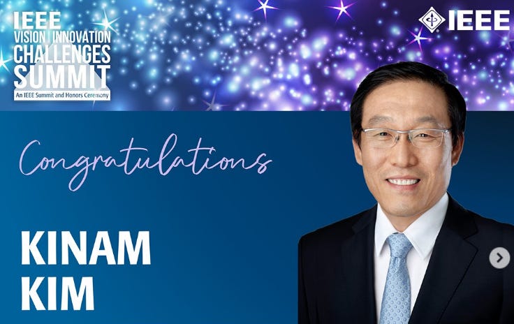
Executive Takeaways
- A Legacy of Market Dominance: Over his 40-plus-year tenure, Dr. Kinam Kim transformed Samsung Electronics from a regional technology follower into an undisputed global leader in memory semiconductors, systematically driving DRAM and NAND Flash to dominant global market shares.
- The 3D V-NAND Pioneer: Dr. Kim’s critical technical and executive oversight led to the commercialization of the world’s first 3D Vertical NAND (V-NAND) in 2013, shattering the physical scaling limits of planar silicon and rewriting the economics of enterprise storage.
- Aggressive Capital Allocation: Under his stewardship, Samsung deployed a counter-cyclical capital expenditure model, leveraging massive capital allocation reserves during industry downturns to out-invest competitors and secure premium valuation multiples during market recoveries.
- The EUV Logic Gamble: Dr. Kim spearheaded Samsung’s early adoption of Extreme Ultraviolet (EUV) lithography in both DRAM and advanced logic foundry nodes, setting the stage for modern high-performance cloud compute architecture and AI accelerators.
The Genesis of a Titan: Entering the Silicon Arena (1981–1990s)
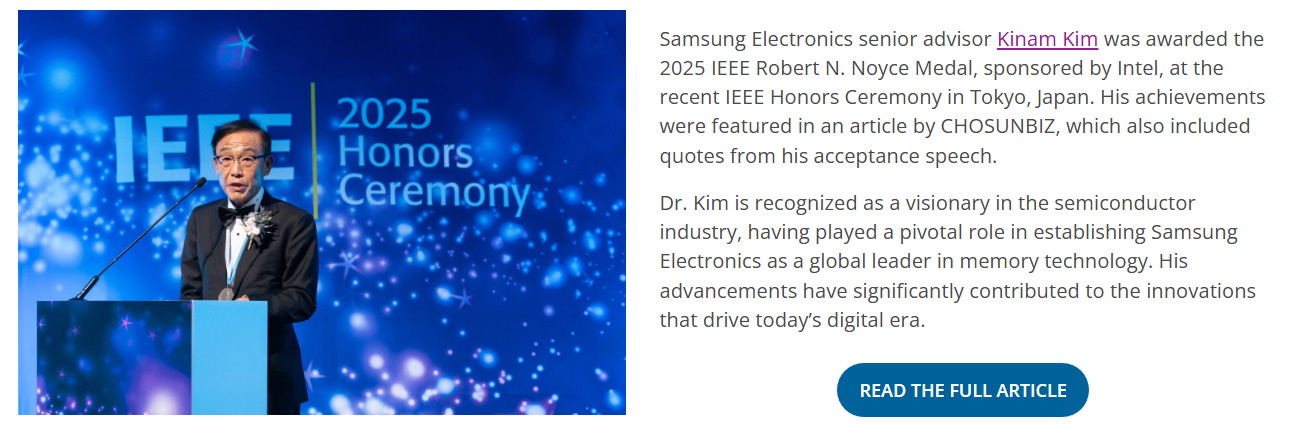
In 1981, a young engineer named Kinam Kim walked into the research facilities of Samsung Electronics. At the time, the global semiconductor landscape was dominated by American pioneers like Intel and Japanese giants like Toshiba and NEC. Samsung was widely regarded as an ambitious but technologically lagging underdog. What followed over the next forty-five years was one of the most extraordinary corporate and technological transformations in industrial history—a narrative of relentless engineering rigor, high-stakes capital allocation, and structural foresight.
Dr. Kim’s early career coincided with Samsung’s high-risk leap into the dynamic random-access memory (DRAM) market. In the 1980s, the company was playing a frantic game of catch-up. Dr. Kim quickly distinguished himself within the R&D division, working on the development of Samsung’s early 4MB and 16MB DRAM chips. This era was defined by razor-thin margins and aggressive price wars. Samsung’s survival depended on achieving yields that competitors could not match, a challenge that required deep expertise in solid-state physics and manufacturing discipline.
By the 1990s, Dr. Kim’s influence had expanded. He became a central architect of Samsung's memory scaling roadmap. His contribution was not merely scientific; it was intensely operational. He recognized that as semiconductor physical dimensions shrank, the traditional methods of lithography and material science would reach a breaking point. Under his technical guidance, Samsung shifted from a strategy of fast-following to one of aggressive, pioneering research, laying the groundwork for the company’s eventual leap to the number-one spot in global DRAM market share in 1992—a position it has held uninterrupted ever since.
The Flash Revolution: Defying Physics with 3D V-NAND
As the computing world transitioned from client-server frameworks to the mobile internet and early cloud compute architecture in the late 2000s, the demand for non-volatile storage skyrocketed. However, the industry was facing an existential crisis: planar (2D) NAND flash memory was hitting a physical barrier. As cell-to-cell spacing shrank below 15 nanometers, quantum mechanical tunneling and electrical interference threatened to render further scaling impossible.
Dr. Kim, then leading Samsung’s Semiconductor R&D Center, made a historic bet. Rather than attempting to endlessly shrink cells horizontally, Samsung would stack them vertically. This conceptual shift from two-dimensional scaling to three-dimensional architecture led to the birth of 3D V-NAND.
The engineering obstacles were immense. Fabricating billions of microscopic, perfectly uniform vertical channels through dozens of active layers required completely new etching processes and chemical vapor deposition techniques. In 2013, under Dr. Kim’s executive leadership, Samsung shocked the technology sector by announcing the commercial production of the world’s first 3D V-NAND flash memory. This breakthrough did not just bypass the physical limitations of planar silicon; it drastically improved write speeds, reduced power consumption, and unlocked unprecedented infrastructure scalability for global data centers.
For enterprise buyers, the introduction of 3D V-NAND redefined the calculation of enterprise ROI. It allowed hyperscale cloud providers to pack petabytes of storage into fractionally smaller physical footprints, fundamentally altering the total cost of ownership (TCO) for data centers worldwide. This technological moat cemented Samsung's pricing power and generated massive market liquidity, which the company immediately funneled back into advanced research and capital expenditure.
The Foundry Crucible: Challenging the Monolithic Duopoly
With the memory business operating as a highly profitable engine, Dr. Kim turned his attention to Samsung’s Device Solutions (DS) Division, which he formally took over as CEO in 2017. His next strategic mandate was highly complex: transform Samsung from a memory powerhouse into a top-tier logic foundry capable of competing directly with Taiwan Semiconductor Manufacturing Company (TSMC).
Under Dr. Kim's direction, Samsung made the bold decision to bypass intermediate optical lithography steps and transition directly to Extreme Ultraviolet (EUV) lithography. EUV technology, utilizing light with a wavelength of just 13.5 nanometers, represented the most complex engineering endeavor in human history. The capital allocation required was staggering; each EUV scanner from Dutch manufacturer ASML cost upwards of $150 million, requiring billions in upfront commitments before a single commercial wafer could be processed.
Dr. Kim understood that this massive capital deployment was essential for long-term risk mitigation. Without EUV capability, Samsung’s sub-7-nanometer and sub-5-nanometer logic nodes would be economically unviable due to multi-patterning defects. By integrating EUV early—not just in logic foundry but also in premium DRAM nodes—Samsung established a dual-track manufacturing advantage. This integration was pivotal for producing the high-bandwidth memory (HBM) and advanced application processors (APs) that power modern artificial intelligence models and high-performance computing platforms.
| Era / Milestone | Key Technology Introduced | Primary Industry Impact | Strategic Financial Outcome |
|---|---|---|---|
| Early 1990s | Sub-micron DRAM Scaling | Secured global #1 spot in DRAM market share (1992). | Established foundation for cash-flow generation and scale economics. |
| 2013 | 3D Vertical NAND (V-NAND) | Overcame planar physical limits; enabled high-density enterprise SSDs. | Drove massive enterprise ROI for hyperscalers; altered data center TCO. |
| Late 2010s | EUV Integration (Logic & DRAM) | Introduced extreme ultraviolet lithography at sub-7nm nodes. | Positioned Samsung as a dual-threat provider of memory and logic. |
| Early 2020s | 3nm Gate-All-Around (GAA) | Transitioned from FinFET to GAA architecture for superior power efficiency. | Protected valuation multiples amidst intensifying foundry competition. |
Industry and Market Implications
Dr. Kinam Kim’s executive decisions have reverberated across the global macroeconomic landscape. His aggressive investment philosophy demonstrated that in the semiconductor industry, conservative capital allocation is often the riskiest path. By maintaining high CapEx through cyclical downturns, Samsung repeatedly forced competitors into defensive consolidations, structurally altering the competitive dynamics of the global tech supply chain.
Who Wins in the Legacy of Kim's Strategy?
- Hyperscale Cloud Providers: Companies operating massive cloud compute architectures have enjoyed a continuous, highly competitive supply of high-density DRAM and solid-state storage, allowing rapid infrastructure scalability without exponential cost increases.
- The AI Ecosystem: Samsung's early integration of advanced lithography set the technological foundation for the mass production of High-Bandwidth Memory (HBM), which is critical to unlocking the memory bandwidth required by modern AI GPU clusters.
- South Korea's High-Tech Economy: Under Kim's leadership, Samsung's semiconductor division became the primary engine of South Korean exports, raising the nation's geopolitical leverage in global supply chain security conversations.
Who Faced Strategic Headwinds?
- Smaller Memory Competitors: Secondary and tertiary memory manufacturers found themselves caught in brutal capital-intensity wars. Those unable to match Samsung's multi-billion-dollar R&D budgets were systematically squeezed out of premium market segments or forced into niche consolidation.
- Late-Adopting Foundries: Foundry players that delayed their EUV transitions found themselves shut out of the sub-7nm logic market entirely, struggling to capture high-margin contracts from top-tier fabless silicon design firms.
Frequently Asked Questions
How did Dr. Kinam Kim’s approach to capital allocation differ from his industry peers?
Unlike many Western executives focused on short-term quarterly earnings and smoothing out capital expenditure to satisfy immediate shareholder demands, Dr. Kim operated on a generational timeline. He utilized a counter-cyclical capital allocation model. When semiconductor prices crashed, Samsung frequently maintained or even increased its capital investments. This strategy ensured that when the market inevitably recovered, Samsung possessed the excess capacity and advanced technology nodes ready to capture maximum market share, driving superior valuation multiples over the full business cycle.
What was the technological significance of transitioning from FinFET to Gate-All-Around (GAA) under his leadership?
As transistors shrank below 3 nanometers, the industry-standard FinFET (Fin Field-Effect Transistor) architecture began to suffer from severe subthreshold leakage current, reducing energy efficiency. Under Dr. Kim's tenure, Samsung pioneered the transition to Gate-All-Around (GAA) nanosheet technology at the 3nm node. By wrapping the gate channel on all four sides, GAA provides vastly superior electrostatic control, reducing power consumption by up to 45% while improving performance by 23% compared to legacy 5nm FinFET processes. This architecture is vital for modern mobile and AI chips demanding extreme thermal and power efficiency.
How did regulatory compliance and geopolitical tensions influence Samsung’s manufacturing footprint during his final years of active leadership?
The intensification of the US-China technology decoupling presented a massive geopolitical challenge for Samsung, which maintained major memory fabrication facilities in Xi'an, China. Dr. Kim oversaw a sophisticated risk mitigation strategy, navigating complex regulatory compliance frameworks including the US CHIPS and Science Act. He balanced these geopolitical pressures by diversifying Samsung’s global manufacturing footprint, greenlighting major investments in advanced logic foundries in Taylor, Texas, while ensuring that legacy facilities in China remained operationally viable under strict international export control parameters.
Future Outlook: What Lies Ahead for Samsung's Semiconductor Division?
As the industry moves deeper into the era of artificial intelligence and quantum computing, the foundation laid by Dr. Kinam Kim will face its ultimate test. The semiconductor landscape of 2026 and beyond is no longer governed solely by physics, but by intense geopolitical alignment and national security concerns.
Samsung's primary challenge in the coming decade is two-fold: maintaining its historical dominance in memory technology against an increasingly aggressive SK Hynix and Micron, and closing the market share gap with TSMC in advanced logic foundry. The rise of High-Bandwidth Memory (HBM4 and HBM5) requires an unprecedented level of co-design between memory architects and logic foundries, making Samsung’s integrated device manufacturer (IDM) model highly advantageous if executed correctly.
Furthermore, the industry is transitioning toward advanced packaging solutions, such as 2.5D and 3D chiplet integration, where multiple dies of varying functions are stacked together in a single system-in-package (SiP). Dr. Kim’s legacy of cross-disciplinary innovation between DRAM, NAND, and logic manufacturing provides Samsung with a unique blueprint to lead this transition. If the company can successfully leverage its integrated capabilities, it will continue to command premium valuation multiples and dictate the tempo of global technology infrastructure for another half-century.