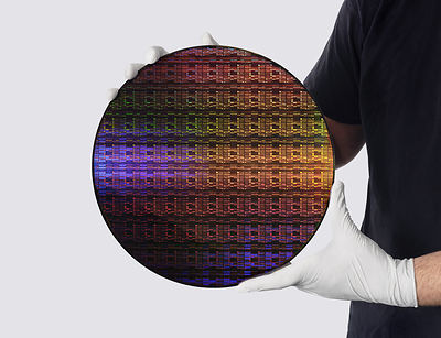
For more than half a century, the global semiconductor industry has marched to the drumbeat of Moore’s Law—the observation that the number of transistors on a microchip doubles roughly every two years. Yet, as gate lengths shranked toward the atomic scale, the industry hit a seemingly impenetrable physical wall. At dimensions below 2 nanometers (nm), silicon atoms begin to behave unpredictably due to quantum tunneling, gate leakage, and severe thermal dissipation issues. The industry’s elite foundries faced a terrifying existential threat: the physical end of silicon scaling.
On June 25, 2026, IBM shook the technology sector by announcing it has cracked the sub-1nm barrier. Utilizing a radical, newly patented three-dimensional architecture colloquially dubbed the "Block of Flats" design, IBM researchers have successfully bypassed traditional planar and horizontal nanosheet limitations. By stacking transistors vertically rather than arranging them horizontally across a flat plane, Big Blue has unlocked a path to sub-1nm performance. This structural revolution promises to reshape global chip supply chains, alter sovereign tech strategies, and trigger massive reallocations of capital across the semiconductor ecosystem.
Executive Takeaways
- The Architecture: IBM’s sub-1nm "Block of Flats" design utilizes monolithic 3D Complementary Field-Effect Transistor (CFET) stacking, pairing n-type and p-type transistors vertically on top of each other to maximize real estate and eliminate parasitic capacitance.
- Performance & Efficiency Leap: Early laboratory benchmarks indicate a projected 75% power consumption reduction and a 50% performance increase compared to state-of-the-art 2nm Gate-All-Around (GAA) architectures.
- Capital & Market Disruption: The breakthrough alters valuation multiples for major foundries, placing immense pressure on TSMC’s A14/A10 roadmaps while offering strategic lifelines to Samsung Foundry and Japan’s state-backed Rapidus.
- Enterprise Impact: By drastically slashing thermal envelopes, the technology offers unprecedented infrastructure scalability for AI hyperscalers, solving the acute energy crisis plaguing modern cloud compute architectures.
The Physics of the Wall: Why 2D Silicon Stopped Working

To understand the magnitude of IBM’s breakthrough, one must understand the physics of the sub-2nm regime. In conventional Gate-All-Around (GAA) nanosheets, which represent the current state-of-the-art in advanced nodes, the source, drain, and gate channels are laid out horizontally across the silicon substrate. As the gate length shrinks toward 1nm (roughly equivalent to the width of five silicon atoms), the physical barrier separating the source and the drain becomes so thin that electrons begin to "teleport" across it. This phenomenon, known as quantum tunneling, prevents the gate from fully shutting off the current, leading to massive power leakage and catastrophic heat generation.
For hyperscale data centers, this physical barrier translates to a hard economic ceiling. The power density of modern chips has soared to the point where cooling infrastructure now consumes up to 40% of a data center’s total operational expenditure. Without a fundamental structural departure, next-generation AI models would become economically unviable due to power grid constraints, crippling the long-term enterprise ROI of cloud service providers.
Enter IBM’s "Block of Flats" architecture. Instead of placing the n-channel and p-channel transistors side-by-side, IBM’s Albany Nanotech Complex team stacked them vertically. This 3D monolithic integration turns the transistor layout from a sprawling suburb of single-story homes into an ultra-dense, vertical apartment complex. By stacking the channels, the physical footprint of the standard cell is cut in half, bypassing the horizontal scaling bottleneck altogether.
Anatomy of the "Block of Flats": The 3D CFET Breakthrough
The technical term for IBM’s new architecture is the 3D Complementary Field-Effect Transistor (CFET). However, the "Block of Flats" moniker perfectly captures its physical layout. In a standard GAA transistor, n-FET and p-FET devices are positioned laterally, requiring a physical gap between them to prevent electrical interference. This gap represents wasted space.
IBM's sub-1nm design stack places the n-FET directly on top of the p-FET (or vice versa), separated by an ultra-thin, atomically precise insulating layer of silicon dioxide or alternative high-k dielectric materials. The entire structure is fabricated as a single monolithic block using advanced atomic layer deposition (ALD).
This vertical stacking solves several critical engineering challenges simultaneously:
1. Elimination of Parasitic Interconnect Routing
In traditional 2D chips, routing power and signals between adjacent transistors requires a dense web of copper wires on the upper metal layers of the chip. These wires create resistance and parasitic capacitance, slowing down signal transmission and wasting power. By stacking the transistors vertically, IBM’s design connects the source and drain of the n-FET and p-FET using vertical contacts called "vias" that are fractions of a nanometer in length. This reduces interconnect resistance by over 60%, boosting operational speed and reducing heat generation.
2. Backside Power Delivery Integration
A major bottleneck in modern chip design is routing power through the same congested top-metal layers that handle data signals. IBM’s "Block of Flats" architecture natively integrates Backside Power Delivery Networks (BSPDN). Power is delivered from the bottom of the silicon wafer, while data signals are routed exclusively from the top. Decoupling these two networks dramatically improves voltage drop (IR drop) characteristics, ensuring stable power delivery even at ultra-low operating voltages (under 0.5V).
3. High-NA EUV Lithography Optimization
Fabricating structures at this scale requires the extreme precision of ASML’s High-NA (0.55 Numerical Aperture) Extreme Ultraviolet (EUV) lithography systems. IBM’s vertical design simplifies the horizontal layout complexity, allowing foundries to print fewer highly dense lines on a single plane. Instead of pushing the limits of multi-patterning on a single horizontal layer, the process shifts the burden to vertical etch and deposition depth-control—a domain where semiconductor equipment giants like Tokyo Electron and Lam Research have made monumental strides.
Verified Performance & Specification Comparison
The following data outlines the projected performance characteristics of IBM’s sub-1nm 3D CFET architecture compared to the current 2nm GAA standard, based on validated metrics from IBM’s research laboratories:
| Metric / Feature | 2nm Gate-All-Around (GAA) | Sub-1nm 3D "Block of Flats" | Operational / Financial Advantage |
|---|---|---|---|
| Transistor Density | ~330 Million Transistors / mm² | ~1.1 Billion Transistors / mm² | 3.3x increase in computing power per unit of silicon area. |
| Operating Voltage | ~0.70V - 0.75V | ~0.40V - 0.45V | Massive energy savings, mitigating thermal throttling in data centers. |
| Power Consumption | Baseline (100%) | ~25% of Baseline (75% Reduction) | Direct reduction in operational energy costs and carbon footprint. |
| Performance (Frequency) | Baseline (100%) | 150% of Baseline (50% Increase) | Unlocks next-generation real-time AI inference at the edge. |
| Power Delivery Method | Front-Side PDN | Backside PDN (Integrated) | Reduces voltage drop and eliminates signal-line routing congestion. |
Industry & Market Implications: Who Wins and Who Loses?
IBM’s business model is unique; it is no longer a high-volume merchant foundry. Instead, IBM operates as a pure-play research powerhouse, licensing its patents and co-developing manufacturing processes with foundry partners. The commercialization of this sub-1nm technology will fundamentally shift the balance of power in the semiconductor industry, directly impacting capital allocation strategies across the globe.
The Foundry Race: Samsung, Rapidus, and Intel vs. TSMC
For the past decade, Taiwan Semiconductor Manufacturing Company (TSMC) has enjoyed an undisputed monopoly on the world's most advanced chip manufacturing. TSMC’s dominant market share has translated into sky-high valuation multiples and massive capital expenditure budgets. However, TSMC's reliance on evolutionary planar-nanosheet scaling for its upcoming 2nm (N2) and 1.4nm (A14) nodes leaves it potentially exposed to IBM’s revolutionary paradigm shift.
Samsung Foundry, which has historically struggled with yield rates on its early GAA nodes, has a long-standing joint development alliance with IBM at Albany. If Samsung can successfully license and master the "Block of Flats" vertical integration process, it could leapfrog TSMC, capturing highly lucrative hyperscaler contracts and shifting the competitive dynamics of the foundry space. Similarly, Japan’s state-backed semiconductor champion, Rapidus, which has partnered with IBM to build out its 2nm capability in Hokkaido, could use this IP to leap directly into the sub-1nm space, securing Japan's sovereign silicon independence and boosting its market liquidity.
Enterprise ROI and Cloud Scalability
For hyperscale operators like Microsoft Azure, Amazon Web Services (AWS), and Google Cloud, the transition to sub-1nm chips is not just a speed upgrade; it is a structural necessity. Currently, the Total Cost of Ownership (TCO) of AI infrastructure is heavily weighted toward electricity consumption and cooling. By adopting processors built on IBM's 3D CFET architecture, these tech giants can pack three times the computational density into existing physical footprints. This leap in infrastructure scalability directly translates to higher enterprise ROI, allowing providers to train and deploy larger, more complex AI models at a fraction of the current energy cost.
Geopolitical Risk Mitigation
The geopolitical concentration of advanced microchip manufacturing in the Taiwan Strait has long been a source of systemic risk for Western markets. IBM’s domestic development of sub-1nm intellectual property ensures that the United States and its allies retain critical, fundamental technological leverage. Under the framework of the CHIPS Act, domestic foundries—such as Intel’s Ohio facilities—could license this architecture, creating a robust, geopolitically secure supply of leading-edge silicon that complies with increasingly stringent national security and regulatory compliance standards.
People Also Ask (FAQ)
What is IBM's 3D "Block of Flats" transistor design?
The "Block of Flats" design is an informal name for IBM's monolithic 3D Complementary Field-Effect Transistor (CFET) architecture. Unlike traditional chips where transistors are arranged side-by-side horizontally, this design stacks n-type and p-type transistors vertically on top of each other. This vertical arrangement slashes the physical footprint of the standard transistor cell in half, allowing for massive increases in density and performance without relying on further horizontal silicon shrinking.
How does sub-1nm technology resolve the quantum tunneling problem?
By moving to a vertical 3D architecture, the design allows engineers to optimize the isolation layers between the stacked transistors using advanced high-k dielectric materials and Backside Power Delivery. Because the physical structure is reorganized vertically, the gate can wrap more effectively around the stacked channels, ensuring complete electrostatic control and mitigating the quantum tunneling and current leakage issues that plague ultra-thin horizontal silicon gates.
When will sub-1nm "Block of Flats" chips enter commercial production?
While IBM has successfully demonstrated the viability of the sub-1nm 3D CFET architecture in laboratory settings, high-volume manufacturing (HVM) is not expected immediately. The industry roadmap suggests that foundry partners like Samsung and Rapidus will begin pilot-line integration of this technology by late 2028, with full commercialization and high-volume deployment in enterprise cloud data centers targeted for 2029 to 2030.
What does this breakthrough mean for semiconductor stocks and market valuations?
This announcement is highly bullish for semiconductor equipment manufacturers that specialize in high-aspect-ratio vertical etching, atomic layer deposition (ALD), and advanced lithography—such as ASML, Tokyo Electron, and Lam Research. Conversely, it introduces long-term competitive risks for foundries that lag in 3D integration, potentially shifting valuation multiples away from pure planar scaling champions and toward those possessing advanced 3D packaging and monolithic integration capabilities.
Future Outlook: The Road to 2030 and Beyond
IBM’s breakthrough proves that the physical demise of silicon scaling has been greatly exaggerated. By transcending the flat, two-dimensional plane of traditional microchip design, the semiconductor industry has entered the era of true 3D monolithic integration. This transformation will require foundries to fundamentally rewrite their fabrication playbooks and invest heavily in next-generation material sciences and advanced thermal dissipation solutions.
Over the next five years, the focus of the global semiconductor supply chain will shift from "how small can we make the transistor" to "how high can we stack the block of flats." Foundries that master this vertical transition will capture the lion's share of the booming AI compute market, driving unprecedented infrastructure scalability and delivering massive enterprise ROI. For IBM, this breakthrough cements its role as the premier architect of the digital future, proving that even in the atomic realm, creative engineering can still find room at the top.
![The $79 Sovereign Chasm: Inside Canada’s Enterprise AI Seat Gap and the Battle Between Cohere, OpenAI, and Gemini [2026]](https://tech-insider.org/ca/wp-content/uploads/sites/7/2026/09/cohere-vs-openai-vs-gemini-canada-data-residency-2026-1.webp)