Executive Takeaways
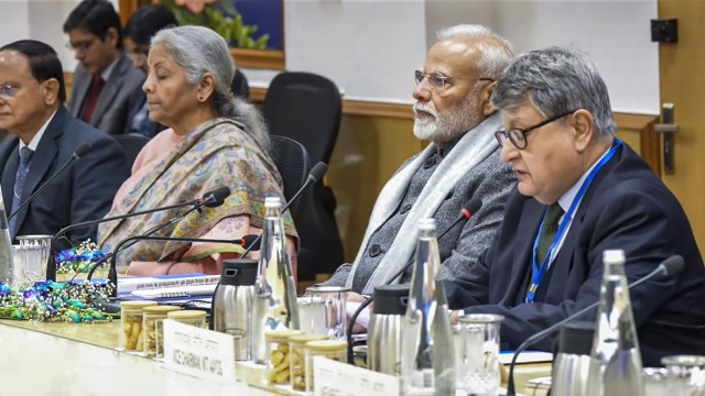
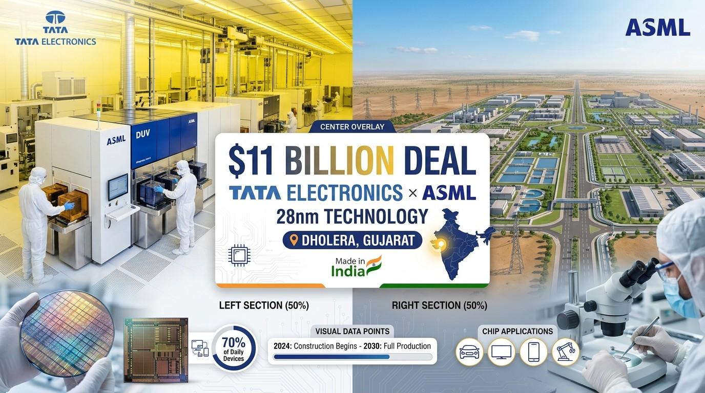
- The Strategic Alliance: On May 16, 2026, a landmark pact between Tata Electronics and ASML, witnessed by the Dutch and Indian Prime Ministers, cemented India’s entry into advanced semiconductor manufacturing.
- Capital Allocation & Infrastructure: Driven by multi-billion-dollar government incentives and aggressive private-equity capital deployment, India is building out the cleanroom facilities, water grids, and power infrastructure required for high-yield fab operations.
- The Lithography Imperative: Securing access to ASML’s advanced lithography systems—the critical path for sub-7nm node scaling—overcomes the primary structural bottleneck facing the Indian semiconductor ecosystem.
- Global Market Realignment: As Western enterprise clients prioritize supply chain diversification and risk mitigation away from single-jurisdiction choke points, India is positioning itself as a viable alternative for high-volume silicon fabrication.
The Hague, May 2026 — When the Dutch Prime Minister and India’s Prime Minister stepped up to the podium on May 16, 2026, to witness the formal signing between Tata Electronics and ASML, the ceremony marked far more than a bilateral trade agreement. It signaled a tectonic shift in the geography of enterprise technology. For decades, the foundational bedrock of the global digital economy—advanced lithography and sub-micron silicon fabrication—remained anchored in a fragile, highly concentrated arc stretching from East Asia to Western Europe. Today, that arc is extending southward.
As corporate balance sheets grapple with macroeconomic volatility and structural supply chain shocks, the race to secure predictable, resilient semiconductor capacity has accelerated. For India, a nation historically dominant in software architecture and IT services yet peripheral to silicon hardware manufacturing, this partnership represents a high-stakes, capital-intensive pivot. Backed by aggressive state-level financial backing and the massive industrial balance sheet of the Tata Group, the partnership with Veldhoven-based ASML addresses the most critical gating item in modern chipmaking: access to extreme ultraviolet (EUV) and advanced deep ultraviolet (DUV) lithography systems.
The Catalytic Convergence: State Policy Meets Industrial Might
Test Our Free AI & Tech Utilities Suite
Calculate LLM API token costs, analyze article dwell-time, or simulate tech DCA returns.
The genesis of India’s modern semiconductor ambitions lies in a calculated convergence of geopolitical risk mitigation and domestic economic policy. For international enterprise buyers, the vulnerabilities laid bare by pandemic-era logistics failures and geopolitical tensions created an urgent imperative for supply chain diversification. In response, the Indian government rolled out the Semicon India program, a multi-billion-dollar fiscal incentive package designed to attract foreign direct investment (FDI) and build domestic technological sovereignty.
Enter Tata Electronics. As the vanguard of the Tata Group’s deep-tech ambitions, the company has methodically assembled a portfolio spanning semiconductor assembly, testing, marking, and packaging (ATMP) facilities in Gujarat and greenfield fab proposals in collaboration with global technology licensors. However, building an advanced logic fab requires navigating a labyrinth of technological dependencies. Without direct access to ASML’s cutting-edge lithography equipment—machines capable of printing features measured in single-digit nanometers using light with a wavelength of just 13.5 nanometers—any domestic fab effort would be dead on arrival.
The May 2026 pact effectively bridges this execution gap. By securing a formalized pipeline for ASML’s advanced semiconductor equipment, Tata Electronics has transitioned from an ambitious regional conglomerate into a credible tier-one contender in the global foundry landscape. This development fundamentally alters valuation multiples and risk assessments for tech investors tracking the region’s hardware infrastructure.
Deconstructing the Engineering and Financial Complexities
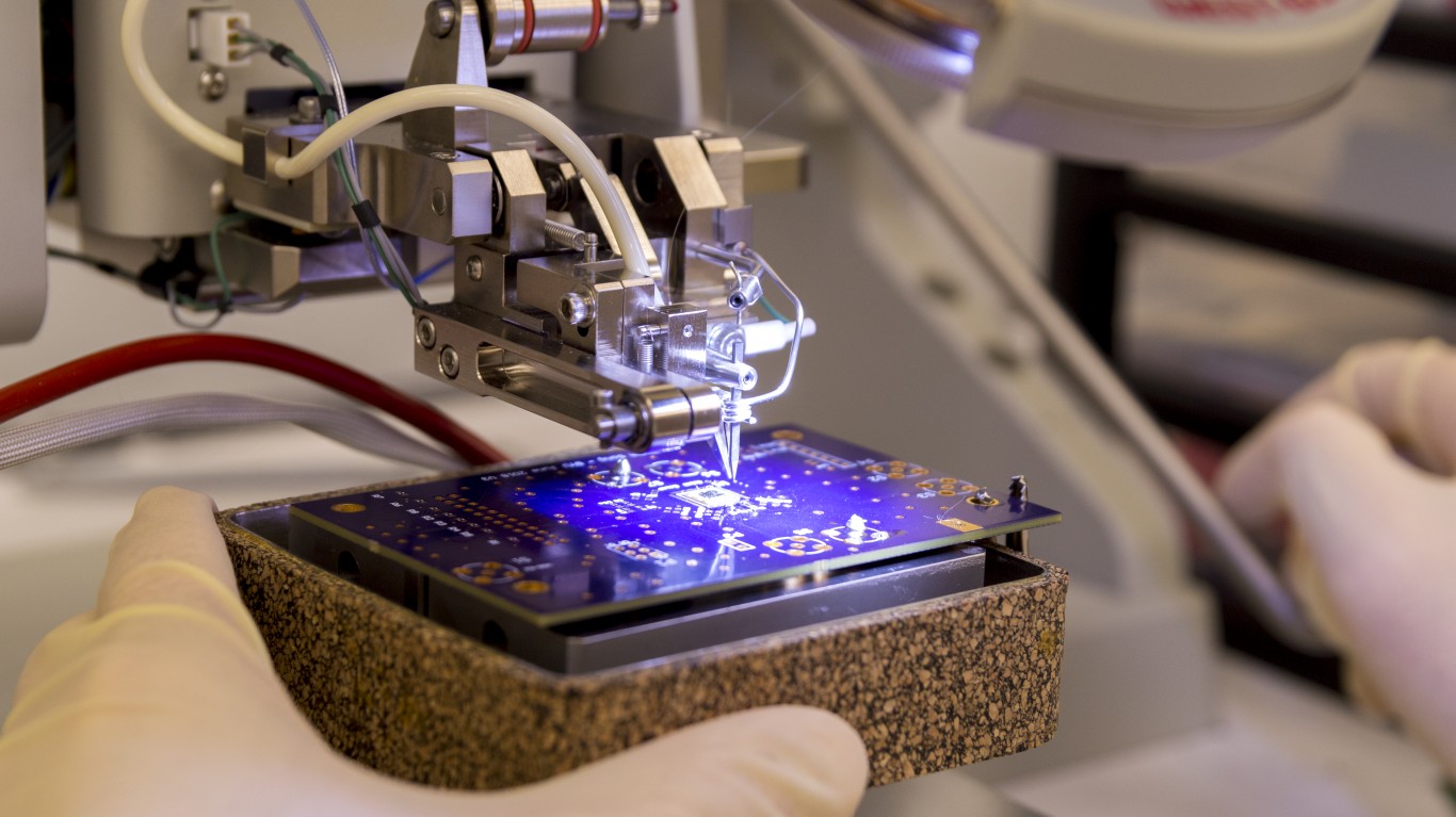
To understand the magnitude of the Tata-ASML partnership, one must examine the staggering economic and physical realities of establishing a semiconductor fabrication plant, commonly known as a fab. A modern logic fab is arguably the most complex manufacturing enterprise ever devised by human engineering, requiring cleanroom environments where air purity is maintained at levels thousands of times cleaner than a hospital operating room.
The capital allocation required is astronomical. Initial capital expenditures for a facility capable of producing advanced nodes routinely exceed $10 billion, demanding meticulous risk mitigation, long-term debt financing, and sustained equity support. Furthermore, fab operations are exceptionally resource-intensive, requiring millions of gallons of ultrapure water and uninterrupted, ultra-stable power grids—infrastructure hurdles that Indian states are currently rushing to resolve through dedicated industrial corridors.
ASML’s role in this ecosystem cannot be overstated. As the sole global monopoly producer of EUV lithography systems, ASML acts as the ultimate tollbooth for advanced silicon scaling. The machinery requires complex cloud compute architecture for real-time calibration, advanced photonics, and highly specialized maintenance teams. By integrating ASML’s supply chain into its domestic roadmap, Tata Electronics is not merely purchasing hardware; it is plugging directly into the upper echelons of global intellectual property and manufacturing precision.
Verified Data & Metrics Breakdown
A comparative analysis of historical Indian technology initiatives versus the current 2026 semiconductor push highlights the unprecedented scale of capital deployment and technological scope:
| Metric / Parameter | Legacy IT / Assembly Era (Pre-2022) | Current Tata-ASML Era (May 2026) |
|---|---|---|
| Primary Focus | Software services, IT outsourcing, basic PCB assembly | Advanced logic fabrication, OSAT, and sub-micron lithography |
| Key Equipment Partner | Standard surface-mount technology (SMT) machinery | ASML (EUV/DUV lithography systems integration) |
| Capital Commitment | Fragmented, largely private-led software investments | Multi-billion-dollar public-private syndication (> $10B+ ecosystem outlay) |
| Regulatory & Compliance Framework | Standard corporate tax laws, IT export incentives | Targeted semiconductor PLI schemes, bilateral Dutch-Indian tech pacts |
Industry & Market Implications: Winners, Losers, and Economic Realignment
The formalization of the Tata-ASML axis sends immediate shockwaves across the global semiconductor value chain, creating distinct winners and losers among institutional investors, equipment suppliers, and enterprise end-users.
- Winners:
- Global Enterprise Buyers: Companies seeking robust supply chain diversification outside of East Asia gain a massive, stable alternative manufacturing hub.
- Specialized Equipment & Materials Vendors: Global chemical, gas, and wafer-handling firms supplying the fab ecosystem will see surging demand for localized inventory.
- The Indian Industrial Base: Domestic engineering firms, specialized construction syndicates, and technical universities will experience a structural boom in high-value employment.
- Losers & Regional Competitors:
- Legacy Regional Foundries: Established smaller players in Southeast Asia lacking access to Tier-1 EUV partnerships risk losing market share in mature-to-advanced node transitions.
- Single-Jurisdiction Dependent OEMs: Consumer electronics and automotive giants slow to diversify their semiconductor sourcing will face margin pressures from more agile, risk-mitigated competitors.
From a macroeconomic perspective, this initiative promises to improve India’s current account deficit over the long term by substituting high-value technology imports with domestic production, while simultaneously anchoring the country firmly within Western-aligned technology security frameworks.
People Also Ask (Frequently Asked Questions)
What is the exact nature of the agreement between Tata Electronics and ASML?
The agreement, witnessed by the Dutch and Indian Prime Ministers on May 16, 2026, establishes a collaborative framework for supplying advanced lithography equipment, technical support, and operational integration for Tata’s upcoming semiconductor fabrication facilities in India. This partnership ensures that Tata Electronics can procure and maintain the sophisticated EUV and DUV systems required to manufacture advanced-node silicon.
How does this partnership impact global semiconductor supply chains?
By introducing a major new manufacturing node in India backed by Western technology standards, the partnership dilutes geographic concentration risks. Global enterprise clients—particularly in the automotive, telecommunications, and consumer electronics sectors—gain a viable, highly scalable alternative for semiconductor sourcing, thereby enhancing global supply chain resilience.
What are the primary hurdles facing India’s semiconductor fab ambitions?
Despite strong government fiscal incentives (PLI schemes) and corporate backing from the Tata Group, the primary challenges remain infrastructural and technical. Operating a sub-micron fab requires uninterrupted, ultra-stable power grids, massive volumes of ultrapure water, and a highly specialized workforce trained in nano-electronics and materials science. Scaling these operational capabilities successfully will dictate the long-term enterprise ROI of the project.
When will commercial silicon production begin from these new Indian fabs?
While cleanroom construction and equipment installation schedules span through 2026 and 2027, initial pilot runs and early-node tape-outs are projected to ramp up toward the latter half of the decade, with high-volume commercial shipments scaling as supporting domestic supply chains mature.
Future Outlook: Milestones to Watch
As the ink dries on the historic Tata-ASML pact, financial analysts and industry observers will be closely monitoring several critical operational benchmarks over the next 12 to 36 months:
- Site Infrastructure Completion: Verification of cleanroom readiness and utility grid stability at Tata’s primary greenfield fab locations.
- Equipment Delivery Schedules: Tracking the physical export and installation timelines of ASML’s advanced lithography systems into India.
- Talent Acquisition & Academic Partnerships: The scale-up of specialized engineering programs designed to train the thousands of PhDs and technicians required to operate a bleeding-edge fab.
- First Silicon Tape-Outs: The successful execution and testing of initial semiconductor wafers, which will serve as the ultimate proof of technical competence for institutional investors and global enterprise clients.
Ultimately, whether India successfully integrates into the premier ranks of the global chip race depends on flawless execution, disciplined capital allocation, and sustained technological collaboration. The alliance with ASML provides the key; it is now up to Tata Electronics to unlock the door.