Executive Takeaways
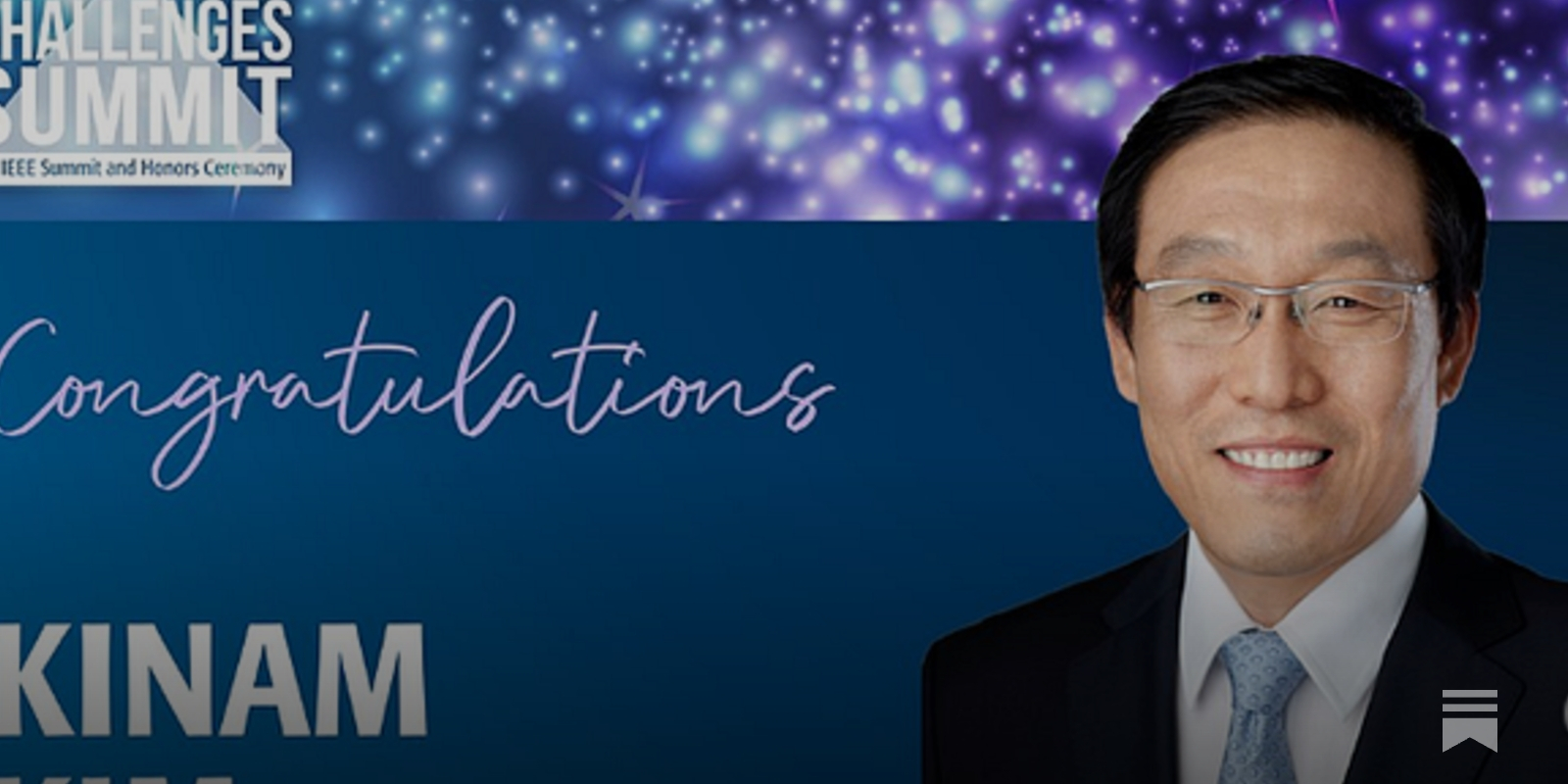
- A Fifty-Year Dynasty: Dr. Kinam Kim’s career spans from Samsung’s infancy in the global microelectronics sector in the early 1980s to his tenure as Chairman of the Samsung Advanced Institute of Technology (SAIT), defining South Korea’s rise to semiconductor hegemony.
- The Paradigm Shifts: Under Kim’s technical stewardship, Samsung pioneered critical leaps from megabit to gigabit DRAM, commercialized the world's first 3D Vertical NAND (V-NAND) in 2013, and spearheaded the aggressive integration of Extreme Ultraviolet (EUV) lithography.
- High-Stakes Capital Allocation: Kim mastered the art of counter-cyclical capital expenditure (CAPEX), utilizing market downturns to build unparalleled infrastructure scalability, forcing competitors out of the market and securing high enterprise ROI.
- The AI Era Frontier: As memory bandwidth becomes the ultimate bottleneck in modern cloud compute architecture, Kim's early R&D laying the foundation for High Bandwidth Memory (HBM) continues to dictate the terms of engagement in the trillion-dollar AI accelerator market.
The Genesis of an Empire: From Fabricating Wafers to Dominating Global Supply Chains
In the early 1980s, the global semiconductor landscape was dominated by an seemingly impenetrable duopoly of American design prowess and Japanese manufacturing precision. When Dr. Kinam Kim joined Samsung Electronics in 1981, the company was widely regarded as a low-cost assembler of consumer electronics, lacking the intellectual property and fabrication precision required to compete at the bleeding edge. South Korea’s semiconductor industry was in its infancy, relying heavily on licensed, lagging-edge technology nodes.
Kim’s entry coincided with Samsung’s audacious decision to enter the ultra-competitive Dynamic Random-Access Memory (DRAM) market. Working inside primitive cleanrooms, Kim and a cohort of highly disciplined engineers embarked on a relentless pursuit of yield optimization and physical scaling. The inflection point arrived in 1983 with the development of the 64Kb DRAM, a project that served as Samsung’s crucible. Kim’s early contributions focused on solving the fundamental materials science challenges of silicon wafer fabrication, developing novel thin-film deposition techniques that minimized defect densities and maximized wafer throughput.
By the early 1990s, the industry faced a critical fork in the road: the transition from trench to stack capacitor designs. While competitors hesitated, weighing the immense financial risks of shifting architectural paradigms, Kim advocated for the stack capacitor method. This engineering gamble proved to be a masterstroke of risk mitigation. It allowed Samsung to stack the capacitor on top of the transfer transistor, optimizing the physical footprint of each cell and dramatically enhancing memory density. Consequently, in 1992, Samsung leapfrogged its global rivals to introduce the world’s first 64Mb DRAM, initiating an uninterrupted thirty-year reign at the apex of the global memory market.
The 3D V-NAND Breakthrough: Defying the Laws of Classical Physics
By the late 2000s, the semiconductor industry was staring into an abyss. Planar (2D) NAND flash memory, the storage medium powering the smartphone revolution and enterprise data centers, was rapidly approaching its physical scaling limits. As cell-to-cell spacing shrank below 15 nanometers, quantum mechanical anomalies—specifically electron leakage and parasitic capacitive coupling—began to compromise data integrity, threatens enterprise ROI, and stall the roadmap of cloud compute architecture.
As the head of Samsung’s Semiconductor R&D Center, Dr. Kinam Kim recognized that horizontal scaling had reached a point of diminishing returns. The solution lay not in drawing narrower lines, but in building upward. In 2013, under Kim's direct leadership, Samsung stunned the technology world by commercializing the world's first 3D Vertical NAND (V-NAND).
This architectural pivot required completely reimagining the physics of charge retention. Samsung transitioned from conventional floating gate technology to Charge Trap Flash (CTF) architecture. Instead of storing electrons in a conductive polysilicon floating gate, CTF utilized a non-conductive, ultra-thin silicon nitride layer to trap electrons safely. Kim’s team developed highly sophisticated Channel Hole Etching techniques, allowing engineers to drill microscopic cylindrical holes through dozens of active wordline layers with high aspect ratios, establishing a uniform vertical channel.
The business implications of this technical triumph were immediate and profound. By bypassing the physical lithography limits of 2D NAND, Samsung unlocked unprecedented infrastructure scalability. The cost per gigabyte plummeted, write endurance multiplied by a factor of ten, and power consumption dropped by half. This technological moat allowed Samsung to capture high-margin enterprise SSD contracts, cementing its dominance among cloud hyperscalers and delivering exceptional returns on research capital.
EUV Lithography and the Foundry Gambit: Forging the Sub-3nm Era
When Dr. Kim assumed the role of Head of the Device Solutions (DS) Division in 2017, he inherited a dual challenge: defending Samsung’s memory hegemony while aggressively expanding its market share in the lucrative pure-play foundry sector, then dominated by Taiwan Semiconductor Manufacturing Company (TSMC). To bridge this gap, Kim executed a highly ambitious, capital-intensive technology roadmap centered around Extreme Ultraviolet (EUV) lithography.
EUV lithography, operating at a wavelength of 13.5 nanometers, represented the most complex engineering endeavor in human history. Implementing EUV required an complete overhaul of cleanroom infrastructure, chemical photoresists, pellicles, and photomask inspection systems. Under Kim's direction, Samsung did not merely adopt EUV for its advanced logic foundry nodes; it became the first in the industry to integrate EUV into its high-volume DRAM manufacturing lines.
This deployment of capital was aimed at securing long-term cost leadership. By utilizing EUV to pattern critical, high-density layers in 14nm-class (D1a) DRAM and below, Samsung eliminated multiple complex deep-ultraviolet (DUV) quadruple-patterning steps. This reduced mask counts, improved manufacturing yields, and accelerated time-to-market. Simultaneously, in the foundry segment, Kim prioritized the development of Gate-All-Around (GAA) transistor architecture—branded as Multi-Bridge Channel FET (MBCFET)—as a replacement for FinFET at the 3nm node. This transition offered cloud providers and fabless chip design houses up to a 45% reduction in power consumption and a 23% performance increase, optimizing the total cost of ownership (TCO) for next-generation AI workloads.
| Era / Milestone | Technical Breakthrough | Strategic Impact | CAPEX & ROI Implications |
|---|---|---|---|
| 1992: 64Mb DRAM Era | Pioneered Stack Capacitor Architecture | Established Samsung as the #1 DRAM manufacturer globally. | High R&D efficiency; initiated long-term memory market dominance. |
| 2013: 3D V-NAND Revolution | Transitioned from 2D Planar to 24-Layer vertical stacking (CTF) | Bypassed physical scaling limits; secured dominant share in enterprise SSDs. | Massive yield advantages; drove down cost per gigabyte below competitors. |
| 2017-2021: EUV & GAA Integration | First to deploy ASML EUV in DRAM; developed 3nm MBCFET | Positioned Samsung Foundry as a premier option for high-performance computing (HPC). | CAPEX exceeded $30B annually; targeted long-term valuation multiple expansion. |
Industry & Market Implications: Who Wins, Who Loses, and the Macro Economics
Dr. Kinam Kim’s five-decade legacy has fundamentally reshaped the geopolitical and macroeconomic landscape of advanced computing. The strategies he pioneered continue to dictate the distribution of market share and influence global capital allocation.
The Winners
- Samsung Electronics & The South Korean Economy: By consistently out-investing rivals during structural downturns, Samsung secured an enduring cash-cow memory business. This steady cash flow subsidizes the capital-intensive foundry division, preserving South Korea's status as an indispensable pillar of the global technology supply chain.
- Cloud Hyperscalers (AWS, Microsoft Azure, Google Cloud): The rapid commoditization and density scaling of DRAM and V-NAND, driven by Kim’s scale-up strategies, dramatically lowered the capital costs of massive data center buildouts, facilitating the rise of SaaS, modern cloud architecture, and generative AI.
- Semiconductor Equipment Manufacturers (ASML, Applied Materials, Lam Research): Samsung's aggressive technological transitions forced the industry to adopt new tooling. This capital spending boom created high-margin revenue streams and immense market liquidity for tier-1 equipment providers.
The Loses
- Legacy Japanese and US Memory Competitors: Companies that failed to match Samsung's rapid capital allocation cycles and technical execution—such as Elpida, Qimonda, and legacy iterations of Toshiba's memory unit—were systematically priced out of the market, leading to bankruptcies, consolidations, or forced joint ventures.
- Late-Entrant Foundry Competitors: The high barrier to entry erected by Samsung’s EUV and GAA investments has effectively locked out smaller, second-tier foundries from competing at advanced nodes, concentrating pricing power in a near-duopoly between TSMC and Samsung.
From a valuation perspective, Kim’s strategic playbook demonstrated that in the semiconductor industry, technology leadership is directly correlated with valuation multiples. Companies that command the leading-edge nodes enjoy superior pricing power during cyclical upswings and resilient operating margins during downturns. This reality has forced contemporary chipmakers to continuously prioritize capital intensity over short-term dividend yields to maintain their market positions.
People Also Ask (FAQ)
Who is Kinam Kim and why is he significant to Samsung?
Dr. Kinam Kim is a legendary South Korean semiconductor engineer and executive who spent nearly five decades at Samsung Electronics. Joining the company in 1981, he rose through the ranks to become the head of the Semiconductor R&D Center, CEO of the Device Solutions Division, and eventually Chairman of the Samsung Advanced Institute of Technology (SAIT). He is widely credited as the chief architect of Samsung's global memory dominance, leading the development of advanced DRAM, the world's first 3D V-NAND, and the integration of EUV lithography.
How did 3D V-NAND solve the physical limits of memory storage?
Prior to 3D V-NAND, flash memory cells were arranged horizontally on a flat plane (2D). As these cells were shrunk below 15nm, they suffered from electron leakage and interference, compromising data retention. 3D V-NAND, commercialized under Dr. Kim in 2013, solved this by stacking memory cells vertically in three-dimensional columns. Utilizing Charge Trap Flash (CTF) technology and high-aspect-ratio etching, Samsung bypassed the physical scaling limits of lithography, dramatically increasing storage capacity, reliability, and power efficiency.
What was Kinam Kim's strategy regarding CAPEX and market cycles?
Dr. Kim executed a highly sophisticated counter-cyclical capital allocation strategy. During industry downturns when competitors scaled back investments to preserve cash, Samsung frequently maintained or increased its Capital Expenditures (CAPEX). This allowed Samsung to construct advanced manufacturing facilities, master new technology nodes, and optimize yields ahead of the competition. When the market inevitably rebounded, Samsung possessed the infrastructure scalability to meet surging demand, capture market share, and maximize enterprise ROI, while competitors struggled to catch up.
What is the significance of Gate-All-Around (GAA) technology in modern foundries?
Gate-All-Around (GAA) is an advanced transistor architecture developed to succeed FinFET at sub-3nm nodes. In a GAA transistor, the gate contacts the silicon channel on all four sides—rather than three sides as in FinFET—minimizing leakage currents, improving electrostatic control, and lowering operating voltages. Under Dr. Kim's leadership, Samsung pioneered this transition with its proprietary Multi-Bridge Channel FET (MBCFET) architecture, offering major performance and power benefits for high-performance cloud compute architectures and AI processors.
Future Outlook: The Road to Sub-1nm and 1,000-Layer Stack
As Dr. Kinam Kim transitions into advisory and emeritus roles, the foundation he established faces a landscape of unprecedented complexity. The semiconductor sector is no longer governed solely by market forces; it is a primary battleground for geopolitical supremacy, governed by strict regulatory compliance, export controls, and supply chain reshoring initiatives.
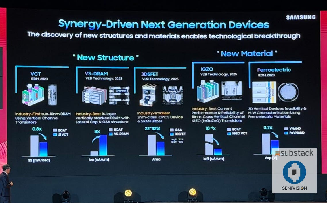
Technologically, the roadmap for the next decade is incredibly ambitious. Samsung is actively working toward stacking V-NAND layers beyond 1,000 layers by 2030, a goal that will require fundamental innovations in high-aspect-ratio etching, new dielectric materials, and wafer-to-wafer bonding. In the DRAM sector, classical physical scaling is approaching its ultimate limits, prompting intensive R&D into 3D DRAM architectures and high-density, low-latency High Bandwidth Memory (HBM4) integrations designed to sit directly on top of AI accelerators.
In the foundry segment, the race to sub-1nm nodes will require the deployment of High-NA (High Numerical Aperture) EUV lithography systems from ASML, alongside backside power delivery networks (BSPDN) to optimize power distribution. The capital requirements for these facilities are staggering, often exceeding $20 billion per fab. The ultimate test of Samsung's post-Kim era will be its ability to balance this massive CAPEX burden with disciplined capital allocation, ensuring that the relentless pursuit of physical scaling continues to yield superior enterprise ROI and market liquidity in an increasingly fractured global economy.