
Executive Takeaways
- Geopolitical Reshoring: Japan has successfully dismantled decades of industrial complacency, funneling tens of billions in public-private capital to reclaim advanced logic fabrication supremacy through Rapidus.
- The 2nm Quantum Leap: Moving past legacy nodes, Japan’s coordinated ecosystem focuses squarely on gate-all-around (GAA) nanosheet architectures to power next-generation enterprise AI, autonomous systems, and hyperscale cloud compute.
- Capital Allocation & Supply Chain De-risking: Global institutional investors are re-evaluating capital allocation strategies, moving away from single-point geographic concentration toward resilient, multi-hub semiconductor infrastructure.
- Market Valuation Shifts: Equipment manufacturers, specialty chemical producers, and advanced packaging foundries across Tokyo's supply chain are experiencing a structural valuation re-rating.
For three decades, the narrative surrounding Japan’s high-tech industry was one of gradual eclipse. Once the undisputed titan of global semiconductor manufacturing in the 1980s—commanding over 50 percent of the world market—Japan watched its domestic fabrication footprint hollow out amidst currency pressures, shifting corporate governance, and the relentless globalization of supply chains led by Taiwan and South Korea. But as global supply chain vulnerabilities, escalating geopolitical flashpoints, and the insatiable computational demands of artificial intelligence converge, Tokyo is orchestrating the most aggressive industrial resurrection in modern economic history.
At the epicenter of this renaissance is a daring bet on 2-nanometer (2nm) semiconductor chips. Spearheaded by the public-private consortium Rapidus—backed by corporate giants like Sony, Toyota, and NTT alongside billions in direct subsidies from the Ministry of Economy, Trade and Industry (METI)—Japan is not merely trying to catch up to the cutting edge. It is attempting to leapfrog legacy limitations to establish a sovereign, highly resilient engine for the next generation of global technological infrastructure. For enterprise CIOs, institutional investors, and sovereign risk analysts, understanding this seismic shift is no longer optional; it is fundamental to long-term risk mitigation and capital deployment.
The Catalytic Turning Point: From Stagnation to Sovereign Urgency
Test Our Free AI & Tech Utilities Suite
Calculate LLM API token costs, analyze article dwell-time, or simulate tech DCA returns.
The genesis of Japan's semiconductor revival was born out of stark realization. The COVID-19 pandemic exposed the fragility of a hyper-concentrated global supply chain. When geopolitical tensions in the Taiwan Strait escalated and fab capacities bottlenecked across East Asia, Japanese automotive lines and industrial automation giants ground to halts not for want of design talent, but for lack of basic, mature-node silicon. More importantly, Japanese leadership recognized that the looming era of generative AI, quantum computing, and edge-intelligence would be dictated entirely by those who control advanced logic nodes.
METI’s strategic pivot departed entirely from historical industrial policy. Rather than shielding domestic champions from foreign competition through protective tariffs, Tokyo adopted an open-architecture, partnership-driven model. By inviting International Business Machines (IBM) and Belgium’s imec into a collaborative nexus, Japan bypassed decades of research-and-development lag. IBM’s breakthrough 2nm nanosheet technology served as the foundational blueprint, which Japanese engineers and advanced equipment suppliers are now aggressively translating into a commercially viable, high-yield manufacturing reality in Hokkaido.
This industrial policy represents a masterclass in modern risk mitigation and public-private capital allocation. By absorbing the initial capital expenditure shock through state backing, Japan has lowered the barrier to entry for private sector conglomerates, creating an aligned enterprise ecosystem capable of competing directly with established foundries in Taiwan and South Korea.
Decoding the 2nm Architecture: Why Nanosheets Change Everything
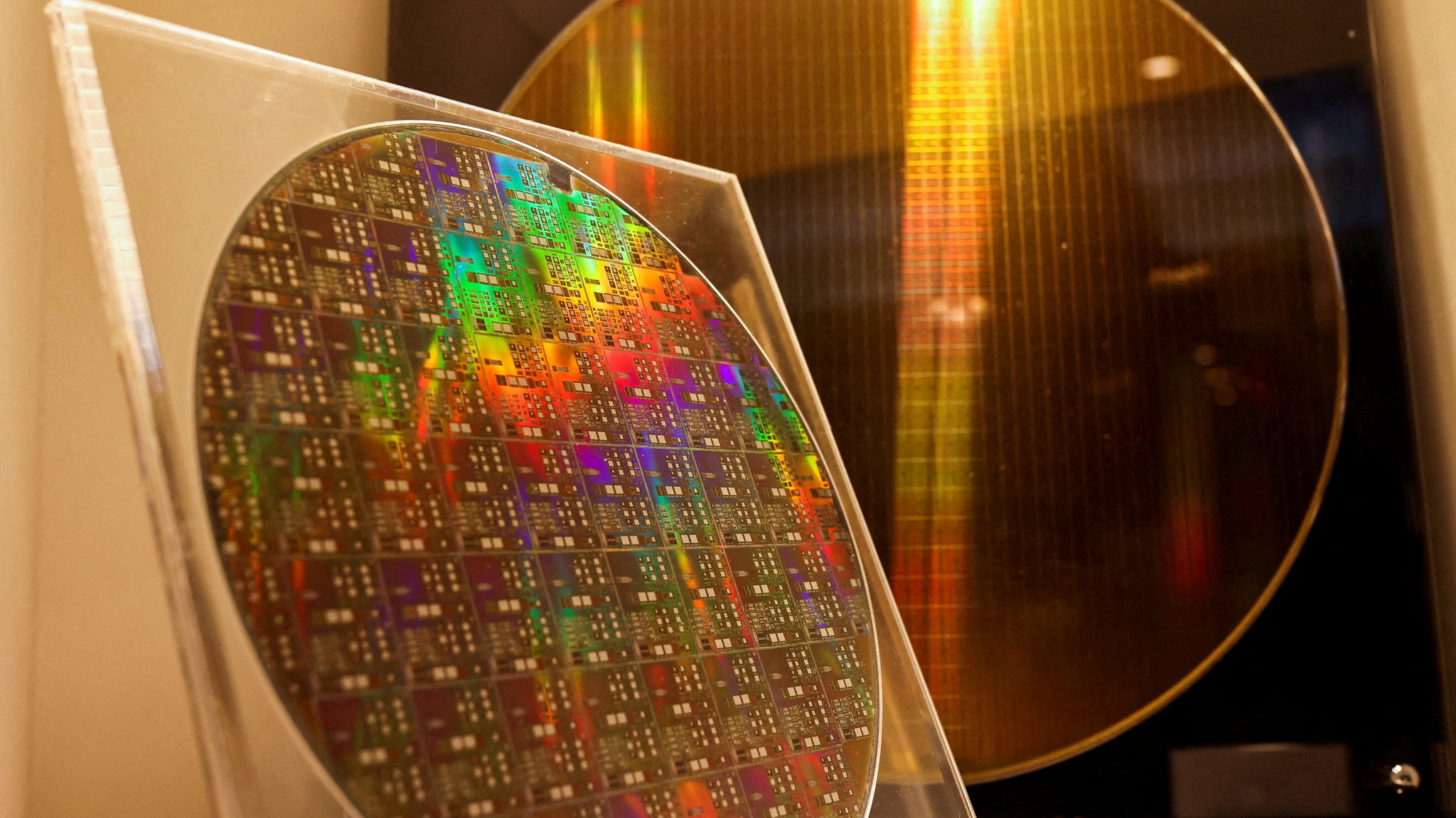
To understand why Japan’s 2nm initiative is capturing the attention of global tech titans, one must examine the physics of sub-3nm silicon. As transistors shrink to the atomic scale, traditional FinFET architectures hit severe electrical performance walls. Current leakage, thermal dissipation, and short-channel effects degrade enterprise ROI and rack-level efficiency in data centers.
The 2nm generation relies on Gate-All-Around (GAA) nanosheet transistors. In this architecture, the gate material surrounds the silicon channel on all four sides, offering vastly superior electrostatic control. For enterprise cloud compute architecture, this translates to:
- Exponential Power Efficiency: Delivering up to 45 percent higher performance at the same power consumption compared to 7nm nodes, or a 75 percent reduction in power use at identical operating speeds.
- Hyper-Dense Transistor Scaling: Packing upwards of 50 billion transistors onto a fingernail-sized die, enabling complex machine learning models to run locally on edge devices without relying exclusively on power-hungry cloud round-trips.
- Thermal Optimization: Mitigating the severe thermal throttling issues plaguing current hyperscale AI accelerators, thereby driving down total cost of ownership (TCO) for enterprise data center operators.
Japan’s unique advantage in this transition does not lie solely in lithography machines—where Dutch giant ASML retains a monopoly—but in the unseen foundational layers: advanced packaging, photoresists, silicon wafers, and extreme ultraviolet (EUV) pellicles. Japanese chemical and material science enterprises control over 50 percent of the global market share for essential semiconductor fabrication materials. By integrating these domestic material strengths directly with Rapidus’s 2nm fab lines, Japan is crafting a vertically integrated ecosystem that minimizes external logistical vulnerabilities.
Verified Data & Metrics Breakdown Table
| Metric / Specification | Legacy 7nm Nodes | Advanced 3nm Nodes | Japan's 2nm Rapidus Target |
|---|---|---|---|
| Transistor Architecture | FinFET | FinFET / Early GAA | Gate-All-Around (GAA) Nanosheet |
| Target Commercialization Date | Fully Commercially Mature (2018–2020) | Active Production (2023–2024) | Pilot Line Operational; Mass Production Targeted 2027 |
| State Subsidy & Capital Commitment | Fragmented / Minimal | Regional Subsidies (CHIPS Act, EU Chips Act) | Over ¥5 Trillion ($30B+) Public-Private Injection |
| Primary Application Focus | Mobile, General Compute | Hyperscale AI, Premium Smartphones | Autonomous Systems, Generative AI, Edge Cloud |
Industry & Market Implications: Winners, Losers, and Valuation Shifts
The ascent of Japan’s 2nm semiconductor ecosystem is triggering a profound re-rating across global financial markets. As institutional capital reallocates to reflect new geopolitical realities, the ripple effects are reshaping multiple sectors:
The Winners: Material Science & Advanced Equipment
Japanese precision equipment makers (such as Tokyo Electron) and advanced chemical conglomerates (such as Shin-Etsu Chemical and JSR Corporation) are experiencing surging valuation multiples. Because 2nm manufacturing requires unprecedented purity and exact molecular tolerances, these foundational suppliers are indispensable. Even if foundries in Taiwan or the US scale 2nm production, they remain fundamentally dependent on Japanese specialty inputs, cementing Tokyo’s indispensable economic leverage.
The Structural Challenge for Incumbents
Established pure-play foundries now face a more crowded competitive landscape. While Taiwan's dominant foundry maintains a commanding market share lead, the emergence of a well-funded, state-backed alternative in Japan introduces geographic diversification that enterprise procurement officers and regulators increasingly demand. Western hyperscalers—looking to de-risk their supply chains away from geopolitical flashpoints—are actively exploring secondary sourcing agreements with Japan.
Macroeconomic Impact & Market Liquidity
Japan’s aggressive fiscal deployment into high-tech infrastructure has revitalized domestic capital markets, driving corporate governance reforms and boosting foreign direct investment (FDI). For investors, Japanese equities tied to automated manufacturing, robotics, and semiconductor supply chains are transforming from cyclical plays into structural growth holdings.
Frequently Asked Questions (People Also Ask)
Why is Japan focusing specifically on 2nm chips instead of trying to catch up at mature nodes?
While Japan has heavily invested in reviving mature nodes (such as TSMC’s Kumamoto fab for 28nm and 12nm automotive chips), the 2nm initiative represents a leap toward future-proofing the economy. Advanced logic chips (2nm and below) are the absolute control points for artificial intelligence, national security systems, and next-generation cloud infrastructure. Capturing the 2nm node ensures Japan remains at the apex of the global technological value chain rather than remaining dependent on foreign advanced logic.
What role does Rapidus play in Japan's semiconductor resurrection?
Rapidus is the central commercial vehicle established in 2022 with backing from major Japanese corporations and massive government subsidies. Its mandate is to leapfrog intermediate nodes and successfully mass-produce 2nm gate-all-around (GAA) logic chips by 2027. Rapidus leverages technological partnerships with IBM and Belgium research institute imec to accelerate its R&D timeline.
How does Japan's 2nm push impact the global supply chain?
Japan’s initiative fundamentally alters the geographic concentration of semiconductor manufacturing. By establishing an advanced fabrication hub in Hokkaido backed by a robust domestic supply chain of chemicals and equipment, global tech enterprises gain a vital alternative sourcing geography, significantly mitigating single-point-of-failure risks associated with East Asian geopolitical tensions.
Are Japanese 2nm chips expected to compete directly with TSMC and Intel?
Yes. Rapidus aims to position itself as an agile, specialized foundry catering to high-performance computing (HPC) and AI clients requiring rapid turnaround times and advanced packaging integration. Rather than competing on sheer volume with industry behemoths, Rapidus is targeting high-margin, time-sensitive enterprise and sovereign applications.
Future Outlook: Milestones and Strategic Horizons to Watch
As the clock ticks toward the targeted 2027 mass-production window for Rapidus, the coming 12 to 24 months will provide critical inflection points for institutional observers and technology executives. Key milestones to monitor include:
- Pilot Line Yield Rates: The successful transition from experimental wafer runs to stable, commercially viable defect densities in the Hokkaido pilot facility.
- Ecosystem Integration: The seamless coupling of Rapidus front-end wafer fabrication with Japan’s burgeoning domestic advanced packaging (3D packaging) initiatives.
- Global Client Acquisition: Securing anchor design wins from major US and European hyperscalers (such as Microsoft, Google, AWS, or Apple) to validate commercial viability.
- Regulatory and Fiscal Continuity: Sustained political commitment and budget allocations from METI regardless of shifting domestic political leadership.
Japan’s 2nm semiconductor strategy is far more than a localized industrial subsidy program; it is a calculated reconfiguration of global technology power. For enterprise leaders navigating a volatile geopolitical landscape, and for investors seeking asymmetric growth opportunities in enterprise infrastructure, Japan's silicon renaissance stands as one of the defining financial and technological narratives of the decade.