Executive Takeaways
- Historical Foundation: India’s semiconductor ambitions are not a modern phenomenon; they trace back to the establishment of the Semiconductor Complex Limited (SCL) in Mohali during the early 1980s.
- Capital Allocation & Scale: Backed by a heavily subsidized $10 billion federal incentive package, the current push has unlocked multi-billion-dollar joint ventures involving Tata Group, CG Power, and global heavyweights like Japan’s Renesas and Taiwan’s PSMC.
- Strategic Risk Mitigation: Amid global geopolitical volatility and supply chain vulnerabilities, global enterprises and sovereign funds are viewing India as a vital diversification node for enterprise ROI and infrastructure scalability.
- Ecosystem Maturation: The shift from legacy state-owned fabrication to commercial logic fabs and Outsourced Semiconductor Assembly and Test (OSAT) facilities signals a comprehensive maturation of the domestic tech ecosystem.
For decades, international observers dismissed India’s semiconductor aspirations as an exercise in industrial nostalgia—a lingering memory of state-led ventures that failed to scale amid global economic liberalization in the 1990s. Today, that narrative is undergoing a radical, high-stakes rewrite. Driven by urgent geopolitical imperatives, aggressive capital allocation, and a fundamental reassessment of global supply chain vulnerabilities, India is executing a calculated pivot from a software-and-services giant to a foundational hardware superpower.
To understand the current multi-billion-dollar influx of capital into Indian silicon, one must look beyond the gleaming press releases of modern megaprojects. The story begins in the agricultural plains of Punjab more than forty years ago, winds through decades of bureaucratic inertia and strategic missteps, and culminates in a modern, highly orchestrated industrial policy designed to secure India’s digital future.
The Genesis: SCL Mohali and the First Wave of Silicon Ambition
Long before global foundries dominated tech discourse, the Indian government recognized the strategic necessity of domestic semiconductor manufacturing. In 1983, Semiconductor Complex Limited (SCL) was established in Mohali under the Department of Electronics. Tasked with designing and fabricating Large Scale Integration (LSI) and Very Large Scale Integration (VLSI) devices, SCL was envisioned as the cornerstone of India’s technological self-reliance.
Initially, SCL achieved notable milestones, producing telecommunication chips and customized microprocessors. However, the enterprise faced severe structural headwinds. Capital expenditure requirements in the semiconductor industry escalate exponentially with every node shrink, and SCL struggled to secure consistent, high-yield funding. A catastrophic fire in 1989 effectively halted production for years, setting the facility back just as the global semiconductor industry was consolidating around advanced CMOS technologies.
Despite its struggles, SCL preserved invaluable institutional knowledge, training a generation of VLSI design engineers who would eventually populate the R&D hubs of Silicon Valley, Bengaluru, and Hyderabad. When the Ministry of Electronics and Information Technology (MeitY) restructured SCL under the Semi-Conductor Laboratory umbrella, it preserved a domestic nucleus for research, even as commercial fabrication shifted to East Asia. SCL’s legacy proved that while India possessed elite-tier chip design talent, it lacked the integrated fabrication ecosystem, regulatory agility, and massive capital reserves required to compete with subsidized Asian foundries.
The Modern Pivot: Incentives, Megafabs, and OSAT Facilities
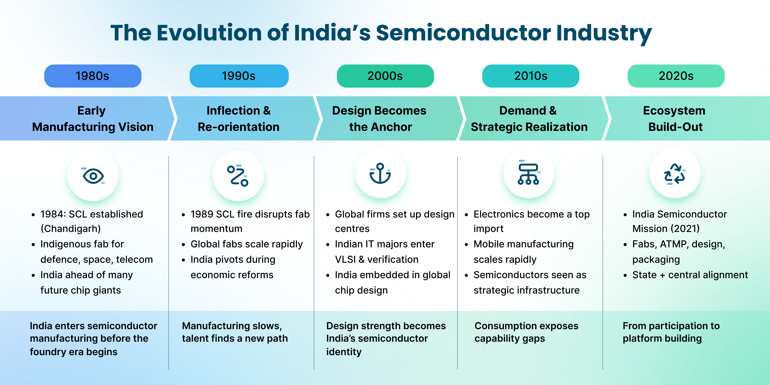
Recognizing that software dominance alone is insufficient for national security and economic resilience, the Indian government launched the Modified Semicon India Programme. Featuring a financial outlay exceeding $10 billion, this initiative was engineered to de-risk capital expenditure for global consortia and domestic industrial titans willing to establish fabrication plants (fabs) and advanced packaging facilities on Indian soil.
Unlike previous iterations, the modern strategy leverages joint ventures and technology transfers. The most prominent among these is the Tata Group’s partnership with Taiwan’s Powerchip Semiconductor Manufacturing Corp (PSMC) to construct a $11 billion commercial logic fab in Dholera, Gujarat. Simultaneously, Tata Semiconductor Assembly and Test (TSAT) is establishing an advanced packaging facility in Morigaon, Assam, addressing the critical downstream bottleneck of backend testing and validation.
Furthermore, CG Power, in collaboration with Japan’s Renesas Electronics and Thailand’s Stars Microelectronics, is investing nearly $1 billion in an OSAT facility in Sanand, Gujarat. These projects are not isolated industrial experiments; they represent a coordinated effort to build a resilient, localized supply chain capable of serving automotive, consumer electronics, and industrial automation sectors.
Verified Data & Metrics Breakdown Table
The following data matrix outlines the primary stakeholders, capital allocations, technological nodes, and projected impacts driving India's semiconductor ecosystem:
| Project / Entity | Location | Capital Outlay (USD) | Technology Node / Focus | Strategic Partner |
|---|---|---|---|---|
| Tata Electronics | Dholera, Gujarat | $11 Billion | 28nm, 50nm Logic Fabs | PSMC (Taiwan) |
| CG Power OSAT | Sanand, Gujarat | ~$790 Million | Advanced Packaging & Testing | Renesas (Japan), Stars Microelectronics |
| Tata TSAT | Morigaon, Assam | ~$3.2 Billion | Flip Chip & Wire Bond Packaging | Independent / Domestic |
| SCL Mohali (Legacy) | Mohali, Punjab | State-Funded | Legacy Nodes & Strategic R&D | MeitY / ISRO Integration |
Industry & Market Implications: Risk Mitigation and Valuation Multiples
The macroeconomic implications of India’s semiconductor push extend far beyond regional industrial development. For global institutional investors, corporate treasuries, and supply chain directors, the transition represents a critical mechanism for risk mitigation. Over-concentration of advanced chip manufacturing in East Asia—particularly Taiwan and South Korea—has long posed a systemic vulnerability for global market liquidity and tech sector valuation multiples.
By establishing geographically diversified manufacturing nodes, enterprises can better protect their cloud compute architecture and hardware supply chains against geopolitical flashpoints. Furthermore, the availability of subsidized capital expenditure and streamlined regulatory compliance makes India an increasingly attractive destination for multinational corporations seeking long-term enterprise ROI.
However, significant challenges remain. Semiconductor fabrication requires immense, uninterrupted supplies of ultra-pure water, stable high-voltage power grids, and specialized chemical supply chains. Ensuring infrastructure scalability across greenfield sites in states like Gujarat and Assam will test the operational execution capabilities of both state governments and private sector partners.
Frequently Asked Questions (People Also Ask)
Why did India’s early semiconductor attempts, such as SCL Mohali, fail to achieve global scale?
Early ventures like SCL Mohali were hobbled by insufficient capital expenditure outlays, rapid technological obsolescence driven by the fast-paced scaling of global nodes, and a debilitating fire in 1989 that halted production. Furthermore, India’s economic environment in the 1980s and 1990s lacked the integrated global supply chains, foreign direct investment inflows, and private-sector partnerships necessary to sustain high-volume commercial fabrication.
How does the modern Indian semiconductor policy differ from past initiatives?
The current Semicon India Programme breaks from historical precedent by offering substantial fiscal support (covering up to 50% of project costs for display and semiconductor fabs) combined with mandatory technology transfer agreements. Instead of relying purely on state-owned entities, the modern framework partners domestic industrial titans like Tata and CG Power with global leaders such as PSMC and Renesas, ensuring immediate access to proprietary process technology and global market channels.
What role do OSAT and advanced packaging facilities play in India's semiconductor strategy?
While front-end fabrication creates the silicon wafers, Outsourced Semiconductor Assembly and Test (OSAT) facilities handle the cutting, packaging, and rigorous testing of integrated circuits. OSAT and advanced packaging represent lower entry barriers with rapid construction timelines, allowing India to rapidly integrate into global semiconductor supply chains while laying the groundwork for more complex logic and memory fabs.
How will India's semiconductor expansion impact global tech valuations and supply chains?
By providing a viable alternative to East Asian manufacturing hubs, India’s semiconductor ecosystem offers critical supply chain risk mitigation for multinational technology firms. This diversification safeguards enterprise ROI, stabilizes market liquidity for hardware manufacturers, and protects cloud infrastructure and automotive supply chains from localized geopolitical disruptions.
Future Outlook: Milestones and Strategic Horizons
As construction progresses across Gujarat, Assam, and other emerging tech corridors, the next 24 to 36 months will serve as the litmus test for India’s industrial strategy. Key milestones to watch include the successful installation of photolithography equipment, the securing of Tier-1 chemical and gas supply chains, and the initial commercial tape-outs from the Dholera fab.
If executed successfully, India’s journey from the pioneering days of SCL Mohali to a globally integrated semiconductor powerhouse will fundamentally reshape the economics of the international tech hardware market. For institutional investors, enterprise executives, and policymakers, monitoring this evolution is no longer optional—it is a core prerequisite for navigating the future of global commerce.