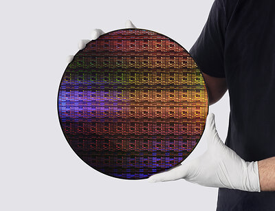
NEW YORK & BENGALURU — In what industry veterans are calling the most consequential hardware breakthrough of the decade, International Business Machines (IBM) has officially unveiled the world’s first sub-1 nanometer semiconductor technology. Announced via the IBM Newsroom on June 25, 2026, the milestone achievement shatters long-held physical limitations in chip manufacturing and promises to fundamentally reshape the economics of global artificial intelligence.
The newly unveiled architecture bypasses traditional scaling bottlenecks by plunging past the elusive 1-nanometer threshold. Utilizing a revolutionary proprietary design, the breakthrough promises to deliver unprecedented computational density while slashing power consumption for hyper-scale AI workloads, cloud data centers, and next-generation consumer electronics.
The Breakthrough: How IBM Defied the Laws of Silicon Physics
For years, semiconductor physicists warned that pushing transistor gates below the 1-nanometer mark would trigger severe quantum tunneling effects—where electrons leak through barriers, causing catastrophic energy loss and thermal instability. IBM’s advanced research and engineering teams have neutralized this threat through the introduction of a radical “nanostack” 3D chip architecture.
Rather than expanding outward on a traditional flat plane, IBM’s sub-1 nm chip leverages vertical integration, allowing current to flow seamlessly through multi-layered nanosheets. This vertical wizardry enables the processor to pack nearly 100 billion transistors onto a piece of silicon no larger than a human fingernail.
- Unprecedented Density: Nearly 100 billion functional transistors on a fingernail-sized die.
- Revolutionary Architecture: Proprietary “nanostack” 3D vertical design routing power efficiently without thermal throttling.
- Quantum-Defense Engineering: Specialized material layers mitigating electron leakage at sub-atomic scales.
- Manufacturing Viability: Designed for compatibility with existing extreme ultraviolet (EUV) lithography ecosystems, lowering barriers to commercial adoption.
Unlocking Massive Power Savings for Generative AI

The timing of IBM’s announcement could not be more critical. As enterprises worldwide race to deploy trillion-parameter generative AI models, global data center energy consumption has surged to alarming levels. Utility grids from Northern Virginia to Frankfurt are straining under the immense electricity demands required to train and run modern Large Language Models (LLMs).
According to preliminary benchmark data released alongside the newsroom briefing, IBM’s sub-1 nm architecture could unlock massive power savings—cutting energy requirements for specific AI inferencing and training tasks by up to 50% compared to current 2nm and 3nm generation nodes.
“IBM’s latest chip breakthrough marks a landmark moment in semiconductor engineering,” noted industry analysts in early responses. “By addressing the existential power wall threatening the AI expansion, IBM has essentially handed the tech sector a vital lifeline for sustainable scaling.”
Market Implications: Wall Street and Global Tech Response
Financial markets reacted swiftly to the June 25 disclosure. Technology equities saw notable shifts as institutional investors weighed the implications of IBM’s leap over competing foundry roadmaps. While major foundries like TSMC, Samsung, and Intel have been aggressively pushing toward 2nm commercialization slated for late 2025 and 2026, IBM’s successful demonstration of a functioning sub-1nm system leaps past immediate industry expectations.
Enterprise clients stand to benefit immensely. Lower power consumption directly translates to dramatically reduced operational expenditures (OpEx) for cloud hyperscalers like Amazon Web Services, Microsoft Azure, and Google Cloud, which spend billions annually on electricity and liquid-cooling infrastructure.
Technical Specifications at a Glance
| Feature / Metric | IBM Sub-1 nm Architecture | Previous Generation (3nm Node) |
|---|---|---|
| Transistor Count | ~100 Billion per fingernail-sized die | ~50 to 60 Billion |
| Primary Architecture | Nanostack 3D Vertical Integration | GAA (Gate-All-Around) Nanosheet |
| Target Application | Trillion-Parameter AI, Cloud Datacenters | General Mobile & Desktop Computing |
| Estimated Power Efficiency | Up to 50% reduction in AI workloads | Baseline standard |
Looking Ahead: The Road to Commercialization
While the initial technical validation has been successfully completed in IBM’s research facilities, the road to mass commercialization remains complex. Scaling the “nanostack” manufacturing process to high-volume commercial foundries will require coordinated supply chain adaptations. However, IBM’s historical playbook—frequently licensing breakthrough semiconductor architectures to global manufacturing partners—suggests that early enterprise pilot chips could begin shipping to select partners within the next 18 to 24 months.
As the AI gold rush continues to demand faster, more efficient silicon, IBM’s sub-1 nanometer debut proves that Moore's Law is far from dead; it has simply evolved into the third dimension.
Frequently Asked Questions
What makes IBM's new chip a "sub-1 nanometer" technology?
The chip utilizes features and gate dimensions measuring strictly below 1 nanometer. By moving beyond traditional planar limits and introducing a 3D "nanostack" architecture, IBM has packed roughly 100 billion transistors onto a single fingernail-sized surface without triggering quantum electron leakage.
How will this impact everyday artificial intelligence applications?
The primary benefit is massive energy efficiency. By cutting power requirements for heavy AI workloads by up to significant margins, companies can run larger, more complex trillion-parameter models faster, cleaner, and at a fraction of current data center cooling and electricity costs.