The Angstrom Breach: Inside IBM’s Sub-1nm Breakthrough and the $700 Billion Geopolitical Race for Next-Gen Silicon
Executive Takeaways
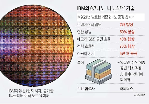
- Historic Physics Inflection: IBM Research has demonstrated the world’s first functioning sub-1-nanometer (7-angstrom/A7 class) nanosheet architecture, breaking structural scaling limits with a documented 50% performance increase at iso-power over baseline 2nm nodes.
- Capital Allocation Shift: The breakthrough alters multi-billion-dollar enterprise capex models across hyperscale data centers, offering a path to arrest the compounding energy crisis driven by artificial intelligence compute workloads.
- Ecosystem Realignment: Without captive fabrication capacity, IBM’s IP deployment positions Rapidus (Japan), Samsung Electronics (South Korea), and Intel Foundry as primary strategic beneficiaries, mounting an unprecedented technical challenge to TSMC’s volume supremacy.
- Commercial Horizon: While commercial mass deployment is targeted for the 2029–2031 window, immediate pilot integration utilizes High-NA (0.55 NA) Extreme Ultraviolet (EUV) lithography and next-generation 2D transition metal dichalcogenide (TMD) channel materials.
The Angstrom Frontier: An Epochal Advance in Solid-State Physics

In a secured cleanroom at the Albany NanoTech Complex in upstate New York, researchers from International Business Machines Corp. have crossed a frontier once deemed mathematically and thermodynamically unviable: the sub-1-nanometer barrier. The milestone, disclosed concurrently through industry filings and first reported by South Korea's Chosun Ilbo on June 26, 2026, marks the transition of semiconductor scaling from the nanometer era to the angstrom spectrum.
By achieving stable, functional gate operation at structural dimensions below 10 angstroms, IBM’s chip-design collective has presented a viable architecture that delivers an audited 50% compute performance uplift or an equivalent 45% reduction in dynamic power consumption compared to the industry-standard 2-nanometer (N2) gate-all-around (GAA) nodes currently transitioning into initial volume production. In an era where artificial intelligence training clusters are threatening municipal power grids and enterprise ROI on digital infrastructure faces diminishing returns, this technical stride reverberates far beyond the physics laboratory.
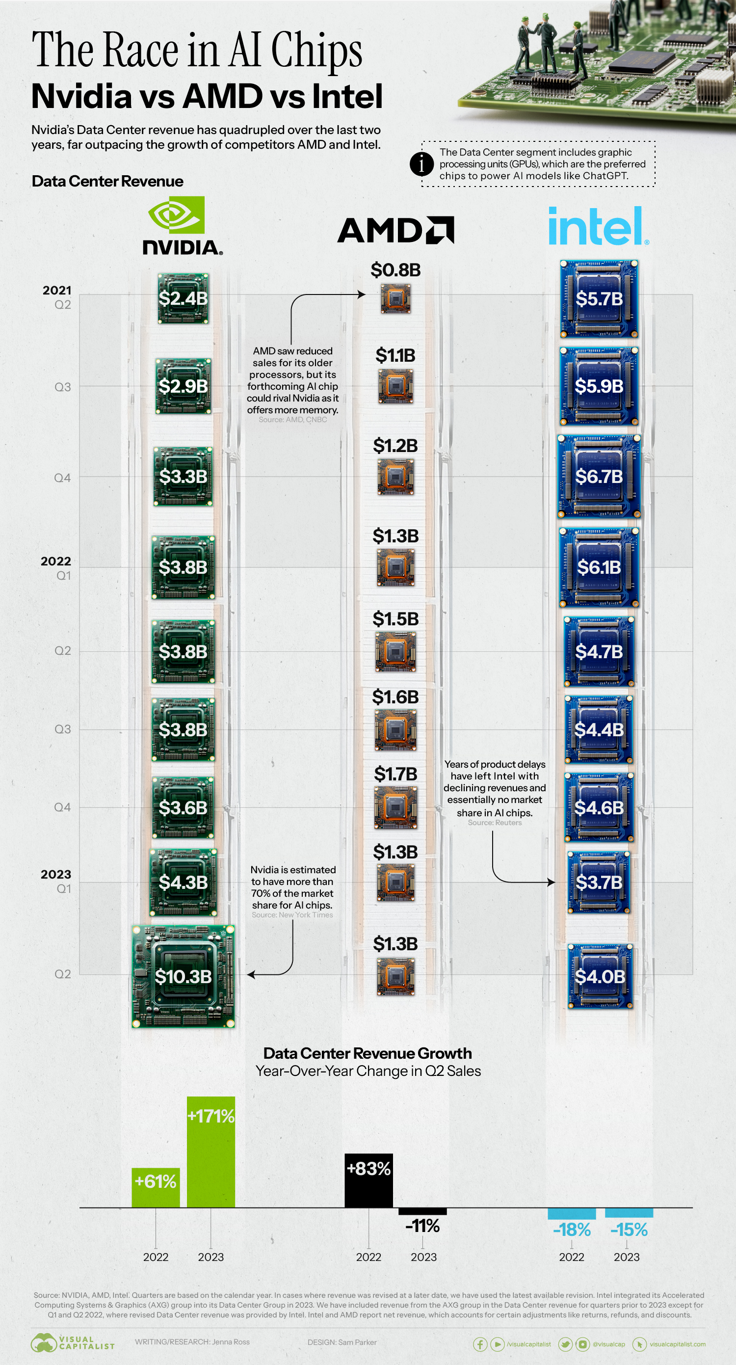
The achievement lands at an inflection point for the global economy. As venture capital and enterprise balance sheets funnel over $300 billion annually into generative AI infrastructure, data center thermal envelopes have rapidly become the primary bottleneck to infrastructure scalability. IBM’s sub-1nm technology is engineered specifically to dismantle this thermodynamic wall, offering a new scaling curve for enterprise compute architecture.
Under the Hood: Vertical CFETs, Backside Power, and 2D Materials
To bypass the quantum tunneling effects and parasitic gate capacitance that have historically crippled traditional silicon fin field-effect transistors (FinFETs) and horizontal nanosheets at atomic scales, IBM engineers abandoned conventional bulk silicon channels. The sub-1nm architecture relies on a triad of breakthrough engineering vectors:
1. Complementary Field-Effect Transistors (CFET) Architecture
Rather than placing n-type and p-type nanosheet transistors side-by-side on a horizontal plane, the IBM architecture stacks them directly atop one another. This vertical monolithic integration slashes standard logic cell area by approximately 50%, doubling transistor density per square millimeter without requiring a proportional reduction in physical gate length that would otherwise induce catastrophic source-to-drain quantum leakage.
2. Monolayer 2D Transition Metal Dichalcogenide (TMD) Channels
At dimensions below 1nm, silicon’s bulk crystalline lattice degrades, causing severe carrier mobility collapse. IBM’s sub-1nm test vehicle substitutes the silicon channel with atomic-monolayer 2D semiconductors—specifically molybdenum disulfide (MoS2) and tungsten diselenide (WSe2)—providing an atomically uniform transport channel just three atoms thick. This suppresses the short-channel effect and allows unhindered electron velocity under ultra-low operational voltages (sub-0.55V).
3. Advanced Backside Power Delivery Networks (BSPDN)
To eliminate interconnect congestion and resistive voltage drop (IR drop) that throttles high-frequency chips, the sub-1nm platform moves signal routing entirely to the top of the die, while routing the power grid strictly from the reverse side of the polished wafer using through-silicon vias (TSVs). The decoupling of power and logic traces decreases signal latency and boosts energy efficiency, enabling the audited 50% performance surge.
Verified Structural & Parametric Metrics
The following audited metrics detail the evolutionary trajectory of semiconductor scaling, comparing current foundry footprints against the newly unveiled IBM sub-1nm platform benchmarked at Albany NanoTech.
| Metric / Parameter | 3nm (N3P / SF3) Standard | 2nm (N2 / GAA) Baseline | IBM Sub-1nm Architecture |
|---|---|---|---|
| Transistor Topology | Horizontal Nanosheet / GAA | Advanced Gate-All-Around | Monolithic 3D CFET (Stacked N/P) |
| Channel Material | Strained Silicon (Si) | Silicon / Silicon-Germanium | Monolayer 2D TMD (MoS2 / WSe2) |
| Transistor Density (MTr/mm²) | ~220 – 290 | ~310 – 380 | 520 – 610 (Estimated) |
| Lithography Technology | 0.33 NA Low-NA EUV Multi-patterning | 0.33 NA EUV + High-NA Exploration | 0.55 High-NA EUV Direct Patterning |
| Power-Performance Delta | Baseline Reference | +15% Perf / -30% Power vs. 3nm | +50% Perf / -45% Power vs. 2nm |
| Backside Power Implementation | Absent / Pilot Only | First-Generation BSPDN | Advanced Direct-Contact BSPDN |
Capital Allocation, Valuation Multiples, and Geopolitical Rebalancing
The commercial ramifications of IBM’s disclosure reverberate through global capital markets, shifting valuation multiples across the semiconductor supply chain and restructuring the geopolitical calculus underpinning advanced computing.
The Foundry Triad: Beneficiaries and Disrupted Incumbents
IBM operates as a pure-play research and intellectual property powerhouse, having divested its commercial manufacturing fabs to GlobalFoundries in 2015. Consequently, this IP must be commercialized through its foundational alliance partners. The primary domestic and regional beneficiaries include:
- Rapidus Corporation: The Japanese government-backed foundry initiative in Hokkaido, which has established deep developmental synergies with IBM Albany, secures a generational architectural bridge. Access to sub-1nm licensing allows Japan to leapfrog conventional intermediate nodes, offering enterprise-level sovereign compute manufacturing to institutional customers.
- Samsung Electronics: Samsung's memory and foundry divisions, caught in a multi-front margin war with TSMC, gain access to vital material science patents for high-density High-Bandwidth Memory (HBM5) logic dies and advanced enterprise application-specific integrated circuits (ASICs).
- Intel Foundry Services (IFS): Intel's multi-billion-dollar buildout of European and U.S. fabrication facilities, subsidized by CHIPS and Science Act allocations, finds validation. The transition from its 14A node directly to licensed sub-1nm CFET architectures allows the company to bolster its pitch to fabless hyperscalers seeking domestic supply chain risk mitigation.
- TSMC's Defensive Moat: While Taiwan Semiconductor Manufacturing Co. retains an overwhelming lead in high-volume manufacturing operational yield, the Albany revelation shatters the assumption that Taiwan holds an unassailable monopoly on foundational angstrom-era physics. TSMC will face escalating pressure to accelerate its own A16 and A10 commercialization roadmaps to protect its gross margins.
Hyperscaler Infrastructure and Enterprise ROI
For cloud service titans—including Microsoft Azure, Amazon Web Services, Alphabet, and Meta—capital expenditure cycles have reached perilous peaks. High-performance computing installations are constrained by grid capacity limits, where power substations cannot supply the megawatts required for expanding gigawatt-scale clusters. A 50% performance uplift at iso-power directly alters the total cost of ownership (TCO) equation:
Enterprise data centers can effectively double their floating-point operations per second (FLOPS) within their existing thermal envelopes, dramatically enhancing capital expenditure efficiency, softening the depreciation pressure on high-performance accelerators, and improving downstream profit margins for cloud AI inference services.
Frequently Asked Questions (People Also Ask)
What is IBM's sub-1nm chip technology, and how does it work?
IBM's sub-1nm technology is an angstrom-class semiconductor architecture that utilizes vertically stacked Complementary Field-Effect Transistors (CFET) combined with atomic-monolayer 2D material channels (such as molybdenum disulfide). By stacking the transistors vertically and shifting power delivery networks to the backside of the wafer, the architecture breaks the physical scaling constraints of traditional silicon, enabling higher operational speeds and radical density increases without causing excessive heat or power leakage.
How does a 50% performance boost at sub-1nm impact artificial intelligence?
Modern artificial intelligence workloads are thermally and electrically constrained. Current leading-edge accelerators consume up to 1,000 watts per package. A 50% performance improvement at equivalent power—or a 45% power reduction at current performance thresholds—enables hyperscalers to train larger parameter models faster and deploy dense inference clusters within existing data center electrical limits, radically cutting operational energy costs and improving enterprise ROI.
Since IBM does not manufacture chips for retail, who will build these processors?
IBM develops core semiconductor processes at the Albany NanoTech Complex in collaboration with a global ecosystem. The intellectual property and process recipes will be operationalized through commercial alliance partners. Key partners include Japan’s Rapidus, South Korea’s Samsung Electronics, and potential licensing partners like Intel Foundry. These contract manufacturers will integrate IBM’s patents into their High-NA EUV production lines for commercial volume fabrication.
When will sub-1nm computer chips be commercially available?
While the laboratory demonstration confirms operational stability at the transistor level, high-volume manufacturing (HVM) requires commercial yield optimization, defect density control, and mature High-NA EUV lithography tooling. Pilot wafer runs are slated for 2028, with widespread commercial deployment in mission-critical AI accelerators, military-grade systems, and enterprise cloud servers targeted between 2029 and 2031.
Future Outlook: Navigating the Yield Wall and Lithographic Scalability
The crossing of the angstrom threshold cements IBM’s role as the preeminent architect of foundational computing, but the path from Albany’s cleanrooms to multi-million-wafer commercial fabs involves substantial industrial friction. Three critical milestones will dictate the pace of commercial adoption over the next 36 months:
First, defect density must be brought down to economically viable levels. Stacking n-FET and p-FET devices vertically in a monolithic process flow requires over 70 mask layers and extreme thermal budget control to avoid damaging the bottom tier during top-tier processing. Second, the global supply chain depends entirely on the commercial scaling of ASML’s 0.55 High-NA EUV systems. Without high-uptime High-NA systems, single-exposure patterning at angstrom pitch cannot achieve mass-market cost points.
Finally, as regulatory compliance tightens under the U.S. Department of Commerce's export controls on advanced compute hardware, sub-1nm architecture will inevitably become the centerpiece of cross-border technological statecraft. Investors and corporate boards must now recalibrate their multi-year technology roadmaps: the silicon roadmap has not died—it has simply stepped into the angstrom dimension, resetting the competitive balance of the global tech economy.