NEW DELHI & CHANDIGARH — Two weeks after initial wires from Konsulteer detailed the tectonic shifts in South Asia’s technology supply chains, a deeper look reveals a decades-long strategic narrative. India’s multi-billion-dollar semiconductor renaissance—characterized by high-profile joint ventures, massive capital allocation, and aggressive government incentives—is frequently mischaracterized as an overnight phenomenon. In reality, today's wafer fabs and advanced packaging facilities are standing on foundations poured more than four decades ago.
As institutional investors, enterprise technology leaders, and geopolitical strategists reassess global risk mitigation and supply chain resilience, India’s semiconductor journey offers a fascinating case study in industrial policy, state-backed enterprise ROI, and long-term infrastructure scalability. From the pioneering yet hobbled Semiconductor Complex Limited (SCL) in Mohali to modern OSAT (Outsourced Semiconductor Assembly and Test) ecosystems taking root in Gujarat and Assam, the subcontinent is attempting a high-stakes leap up the value chain.
Executive Takeaways
- Historical Roots: India’s semiconductor ambitions originated in the 1980s with the founding of the state-run Semiconductor Complex Limited (SCL) in Mohali, laying early groundwork despite bureaucratic and capital hurdles.
- Massive Capital Allocation: Backed by a $10 billion fiscal incentive package (Semicon India program), the country has successfully attracted multi-billion-dollar greenfield projects from global powerhouses like Micron, Tata Electronics, and CG Power.
- Beyond Fabs: Recognizing the prohibitive costs and immense water/power requirements of leading-edge logic fabs, India is strategically prioritizing advanced packaging, OSAT facilities, and indigenous chip design via the Design-Linked Incentive (DLI) scheme.
- Market & Valuation Implications: While enterprise ROI and infrastructure readiness face short-term regulatory compliance and supply chain bottlenecks, successful execution could rewrite global valuation multiples for Indian electronics and manufacturing conglomerates.
From State-Led Pioneer to Global Ecosystem: The SCL Genesis
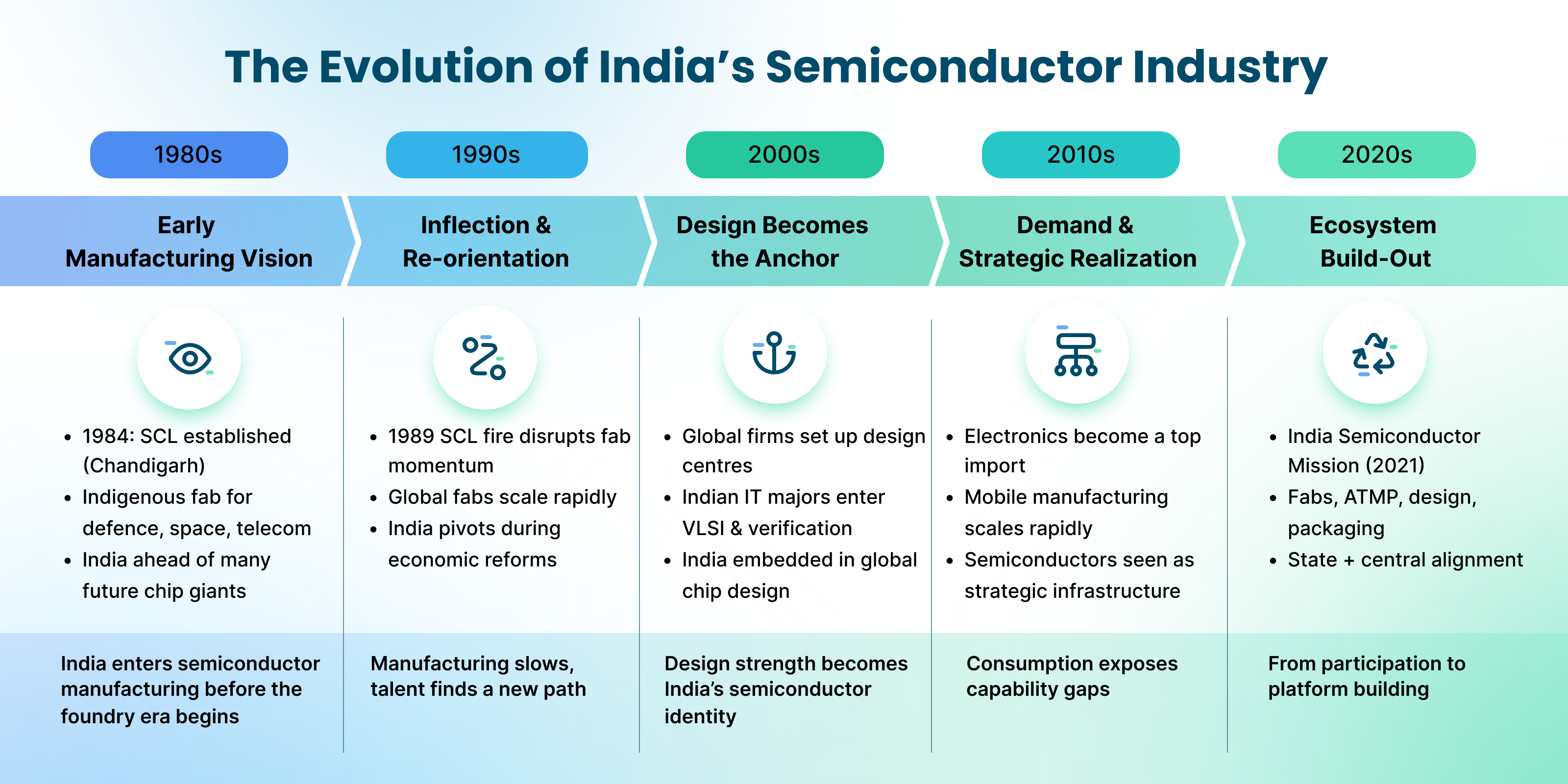
To understand the current architecture of India’s chip ambitions, one must examine the geopolitical and economic landscape of the early 1980s. Established in 1983 under the Department of Electronics, Semiconductor Complex Limited (SCL) in Mohali, Punjab, was envisioned as India’s crown jewel in high-tech manufacturing. Armed with foreign technology transfers and ambitious blueprints, SCL was designed to produce Large Scale Integration (LSI) and Very Large Scale Integration (VLSI) devices primarily for telecommunications and strategic sectors.
However, SCL’s trajectory underscores the classic hazards of early state-led capital allocation without a mature domestic vendor ecosystem. In 1989, a catastrophic fire destroyed SCL’s fabrication facility, effectively setting the national semiconductor program back by a decade. Protracted bureaucratic delays, a lack of continuous venture funding, and rapidly evolving global semiconductor lithography standards made it difficult for SCL to keep pace with Moore’s Law. While the facility survived—eventually coming under the aegis of the Indian Space Research Organisation (ISRO) as Semi-Conductor Laboratory to cater to domestic space and defense needs—it operated in a silo, detached from the hyper-competitive global commercial market.
Despite these historical bottlenecks, SCL served as an invaluable talent incubator. Generations of Indian microelectronics engineers, VLSI architects, and process specialists trained within its cleanrooms before migrating to Silicon Valley, Taiwan, and Europe. This diaspora would ultimately form the intellectual capital driving modern multinational semiconductor design centers in Bengaluru, Hyderabad, and Pune.
The Modern Pivot: The $10 Billion Semicon India Gamble
Fast forward to the post-pandemic era, where acute supply chain shocks, geopolitical friction in the South China Sea, and the imperative for supply chain diversification forced a radical policy pivot in New Delhi. Recognizing that software prowess alone could not insulate the domestic economy from global hardware shortages, the Indian government launched the comprehensive Semicon India program, backed by a robust $10 billion fiscal outlay designed to co-fund semiconductor fabs, display fabs, and compound semiconductor facilities.
This aggressive financial incentive structure—offering up to 50% fiscal support for capital expenditures—has fundamentally shifted enterprise risk calculations for global chipmakers. The strategy is no longer about attempting to immediately rival Taiwan Semiconductor Manufacturing Company (TSMC) at the 2-nanometer leading edge. Instead, a pragmatic, phased roadmap has been deployed:
- OSAT and Advanced Packaging: Recognizing that modern processors rely heavily on heterogeneous integration and advanced packaging (such as 2.5D/3D stacking and chiplets), India has attracted major investments in assembly and test operations.
- Mature-Node Fabs: Targeting 28nm to 65nm nodes—which power everything from automotive microcontrollers and IoT devices to power management ICs and industrial automation systems—ensures immediate utility for high-growth sectors.
- Compound Semiconductors: Focusing on Silicon Carbide (SiC) and Gallium Nitride (GaN) for electric vehicle (EV) power trains, renewable energy infrastructure, and 5G/6G telecom networks.
A prime beneficiary of this policy momentum is Micron Technology’s $2.75 billion assembly and test facility in Sanand, Gujarat. By breaking ground at record speed and leveraging state subsidies, Micron is pioneering a blueprint that other multinationals are closely monitoring for valuation multiples and operational scalability.
Verified Data & Metrics Breakdown
The following data matrix outlines the evolution and current landscape of India’s semiconductor milestones, contrasting historical constraints with modern industrial policy metrics:
| Parameter | Historical Era (SCL Mohali, 1980s–1990s) | Modern Era (Semicon India, 2020s–Present) |
|---|---|---|
| Primary Focus | Defense, Telecommunications, Space Research | Commercial OSAT, Mature Nodes, EV Power, Design |
| Capital Allocation | Modest, centralized public sector outlays | $10 Billion+ incentive package (50% direct fiscal support) |
| Technology Nodes | Legacy bipolar and early CMOS (micron-scale) | 28nm to 65nm logic, advanced packaging & chiplets |
| Private Sector Participation | Virtually nonexistent (state monopoly) | Major conglomerates (Tata, CG Power) + Global Giants (Micron) |
| Talent Ecosystem | Isolated domestic talent pool | Global diaspora integration, 85,000+ targeted specialized engineers |
Industry & Market Implications: Winners, Losers, and Economic Realities
The institutional restructuring of India’s semiconductor landscape triggers profound ripple effects across global financial markets, corporate boardrooms, and regional economies.
The Winners
Domestic Conglomerates & Joint Ventures: Firms like Tata Electronics—which is constructing a multi-billion-dollar fab in Gujarat in partnership with Taiwan’s Powerchip Semiconductor Manufacturing Corp (PSMC)—are positioned to capture immense enterprise value. By integrating semiconductor manufacturing with their existing automotive, electronics, and telecommunications portfolios, these conglomerates are building formidable economic moats.
Global Equipment & Material Suppliers: Applied Materials, Lam Research, ASML, and specialized chemical providers stand to gain significantly as greenfield cleanrooms require billions of dollars in wafer fabrication equipment (WFE) and specialty gases.
The Challenges & Vulnerabilities
Despite bullish market projections, significant operational hurdles remain. Semiconductor manufacturing is hyper-intensive in its consumption of ultra-pure water, uninterrupted power, and toxic chemical handling. Infrastructure scalability in states like Gujarat and Assam requires massive municipal and state-level investments to prevent operational bottlenecks.
Furthermore, regulatory compliance, intellectual property protection, and the velocity of talent acquisition will dictate whether these greenfield sites achieve profitable unit economics. While the government absorbs a massive portion of the initial capital expenditure risk, long-term commercial viability will rest on sustained yield rates and global market pricing stability.
Frequently Asked Questions (People Also Ask)
1. Why did India’s early semiconductor efforts, like SCL Mohali, fail to scale globally?
SCL Mohali faced severe setbacks, notably a destructive fire in 1989 that halted operations for years, combined with a lack of continuous venture capital, rapidly shifting global lithography standards, and a nascent domestic electronic component market. While it successfully served India's strategic space and defense sectors, it lacked the commercial agility and massive capital infusions required to compete with burgeoning East Asian foundries.
2. What is the total financial outlay of the current Semicon India initiative?
The Indian government has committed an initial fiscal outlay of $10 billion (INR 76,000 crore) specifically targeted at incentivizing semiconductor and display manufacturing ecosystems, offering up to 50% of project cost subsidies for greenfield fabs and OSAT facilities.
3. Is India manufacturing advanced leading-edge chips (like 2nm or 3nm)?
Currently, no. India’s immediate strategic focus is on mature nodes (28nm to 65nm), compound semiconductors (SiC/GaN), and advanced packaging/OSAT facilities. This approach aligns with global demand for automotive, industrial, and IoT applications while building foundational supply chain expertise before attempting leading-edge logic fabrication.
4. How does the Design-Linked Incentive (DLI) scheme benefit startups?
The DLI scheme provides financial support and deployment-linked incentives across various stages of integrated circuit (IC) and chipset design. It covers up to 50% of eligible expenditure and offers deployment incentives to domestic fabless startups, fostering an indigenous intellectual property ecosystem.
Future Outlook: Critical Milestones to Watch
As the first wave of modern Indian semiconductor plants transitions from groundbreaking ceremonies to equipment installation and trial production over the next 18 to 36 months, financial analysts and industry observers will monitor several key performance indicators:
- Yield Rate Benchmarks: The speed at which newly operational OSAT facilities and mature-node fabs achieve commercial-grade yield rates will determine their global competitiveness.
Ecosystem Localization: The arrival of Tier-1 and Tier-2 chemical, silicon wafer, and precision equipment suppliers within close geographic proximity to the new fabs in Gujarat and Tamil Nadu.
- Talent Pipeline Execution: The success of specialized academic-industrial partnerships designed to train over 85,000 semiconductor engineers under the federal Chips-to-Startups (C2S) program.
India’s semiconductor story has evolved from an isolated state-led experiment in Mohali to a core pillar of global tech diversification. While formidable structural challenges remain, the combination of aggressive capital allocation, geopolitical tailwinds, and deep engineering talent ensures that the subcontinent is no longer just a consumer of silicon, but an active, indispensable architect of the future global hardware economy.