ALBANY, N.Y. — In the sterile confines of the Albany NanoTech Complex, a quiet milestone was achieved that is poised to fundamentally alter the valuation multiples, capital allocation strategies, and technological roadmaps of the global semiconductor industry. IBM Research unveiled the world’s first functional 2-nanometer (nm) node test chip, packing a staggering 50 billion microscopic switches onto a piece of silicon no larger than a fingernail.
This landmark breakthrough, announced on May 6, 2021, represents a seismic shift in enterprise compute architecture and physical science. As global enterprises grapple with soaring cloud compute costs, escalating energy grids, and stringent ESG regulatory compliance, IBM’s nano-scaling architecture offers a direct counter-strategy to the looming physical death of Moore’s Law. For institutional investors, hedge funds, and enterprise tech executives, understanding the cascading market liquidity and supply chain ramifications of this announcement is no longer optional—it is a critical imperative for long-term risk mitigation.
Executive Takeaways
Test Our Free AI & Tech Utilities Suite
Calculate LLM API token costs, analyze article dwell-time, or simulate tech DCA returns.
- Unprecedented Density: IBM’s 2nm test chip integrates 50 billion transistors on a footprint the size of a fingernail, achieving a density of 333 million transistors per square millimeter.
- Efficiency Gains: The new architecture delivers a projected 45% increase in performance or a 75% reduction in power consumption compared to standard 7nm node production chips.
- Enterprise ROI Transformation: Data centers utilizing 2nm-class processors can anticipate dramatic reductions in cooling overhead and power usage, directly accelerating infrastructure scalability and lowering total cost of ownership (TCO).
- Geopolitical & Foundry Dynamics: While IBM designs and prototypes at its Albany research hub, the commercialization race heavily involves foundries like TSMC, Samsung, and Intel, altering global semiconductor supply chain dependencies.
Comprehensive Narrative: The Architecture of Sub-Microscopic Scaling
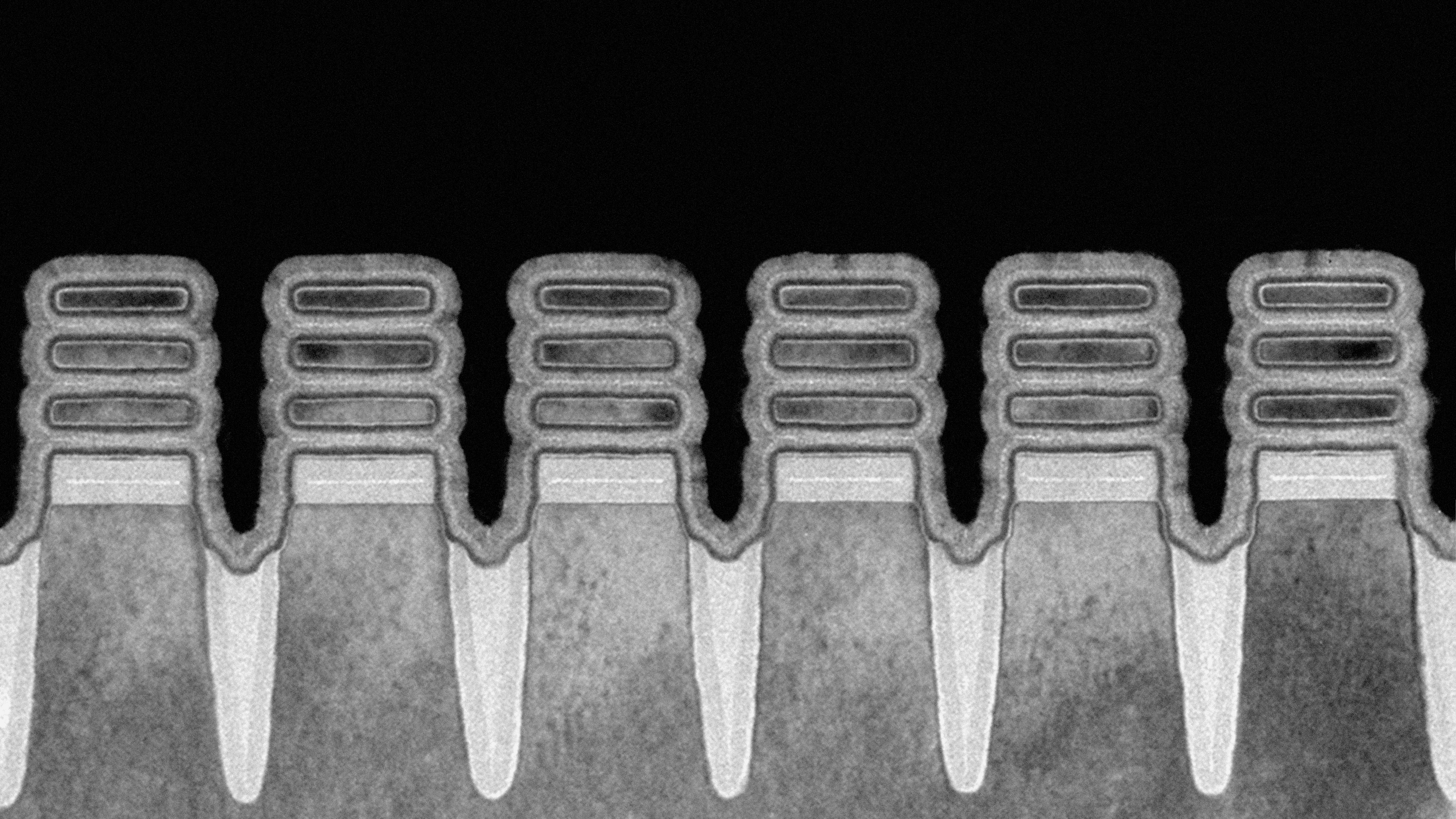
For decades, the semiconductor industry has marched to the rhythmic cadence of Moore’s Law—the observation that the number of transistors on a microchip doubles roughly every two years. However, as fabrication nodes shrunk past 10nm and into the single-digit nanometer realm, quantum tunneling effects and severe leakage currents began to threaten the viability of traditional FinFET (Fin Field-Effect Transistor) architectures. Electrons began leaking through barriers, generating excessive heat and rendering further scaling economically unviable.
IBM Research bypassed this fundamental physics bottleneck by pioneering nanosheet gate-all-around (GAA) technology. Rather than relying on traditional vertical fins, IBM’s design utilizes stacked horizontal nanosheets of silicon. This geometry allows the gate material to completely wrap around the channel on all four sides, offering superior electrostatic control and virtually eliminating current leakage.
"The IBM breakthrough in 2nm technology is at the very heart of society and technology," said Dr. Darío Gil, Senior Vice President and Director of IBM Research, during the unveiling. "It gives our industry the cutting-edge capabilities needed to tackle the toughest challenges in enterprise computing, artificial intelligence, cloud architecture, and beyond."
The manufacturing complexity required to fabricate features measured in mere angstroms cannot be overstated. Developing a 2nm node demands extreme ultraviolet (EUV) lithography systems capable of etching patterns with light wavelengths of just 13.5 nanometers. Achieving a yield rate high enough to successfully pattern 50 billion functional transistors on a single die validates decades of capital expenditure in research and development, proving that silicon scaling still has significant runway left before hitting a terminal thermodynamic wall.
From an enterprise ROI perspective, the implications are profound. Mobile devices powered by 2nm architecture could theoretically achieve a fourfold battery life extension, requiring users to charge their smartphones only once every four days. Simultaneously, hyper-scale cloud data centers—the nerve centers powering global financial transactions, AI model training, and enterprise SaaS platforms—stand to save billions of dollars in electricity and liquid-cooling infrastructure costs.
Verified Data & Metrics Breakdown Table
| Metric / Specification | Standard 7nm Node | IBM 2nm Test Chip Node | Comparative Advantage / Impact |
|---|---|---|---|
| Transistor Density | ~90 to 100 million transistors / mm² | ~333 million transistors / mm² | Approx. 3.3x increase in transistor packing density. |
| Total Transistor Count | Varies by die size (typically 10B–30B) | 50 billion transistors | Unprecedented compute capability per square millimeter. |
| Performance Gain (at same power) | Baseline | +45% Performance Improvement | Substantial speedup for complex AI workloads and database queries. |
| Power Reduction (at same perf.) | Baseline | 75% Lower Energy Consumption | Drastic reduction in data center cooling requirements and operating expenses. |
| Architectural Foundation | FinFET Architecture | Nanosheet Gate-All-Around (GAA) | Enhanced gate control, mitigating quantum leakage currents. |
| Announcement Date | Various (Industry-wide adoption ~2019) | May 6, 2021 | Marks the official laboratory validation of the 2nm milestone. |
Industry & Market Implications: Capital Allocation and Foundry Warfare
The unveiling of IBM’s 2nm test chip reverberated far beyond academic and R&D circles, instantly triggering strategic realignments across global technology markets. In the hyper-competitive semiconductor foundry market, leadership at the leading-edge node dictates pricing power, gross margins, and customer acquisition. Companies that control sub-3nm manufacturing capabilities dictate the hardware roadmaps for hyperscalers like Amazon Web Services, Microsoft Azure, Google Cloud, and Apple.
For investors, evaluating valuation multiples in the semiconductor sector requires a nuanced understanding of capital intensity. Building and equipping a modern semiconductor fabrication facility (fab) capable of producing 2nm chips requires multi-billion-dollar capital expenditures. While IBM historically transitioned away from volume manufacturing—outsourcing its production lines to partners like Samsung—its research consortia model enables foundational intellectual property (IP) licensing that cascades down to major foundries.
Who Wins:
- Hyperscale Cloud Providers: Facing relentless demand for generative AI, large language models (LLMs), and high-frequency financial modeling, cloud giants will secure massive efficiency gains, driving down cost-per-compute metrics.
- Foundry Leaders: TSMC, Samsung Foundry, and Intel Foundry Services stand to capture extraordinary market share as they transition IBM’s nanosheet innovations from laboratory test chips into high-volume commercial manufacturing lines.
- EDA and IP Vendors: Electronic Design Automation (EDA) giants like Synopsys and Cadence benefit immensely as chip designers require entirely new software toolsets to model and verify complex nanosheet gate-all-around architectures.
Who Loses:
- Legacy Chipmakers Lacking R&D Scale: Competitors unable to fund the transition from FinFET to GAA architectures risk structural obsolescence in high-performance computing (HPC) and premium mobile segments.
- Energy-Inefficient Data Center Operators: Operators locked into legacy cooling and older generation nodes will face severe margin compression as power grids strain and energy pricing volatility increases.
Frequently Asked Questions (People Also Ask)
What is a nanometer (nm) in the context of semiconductor manufacturing?
In semiconductor nomenclature, the nanometer rating (such as 7nm, 5nm, or 2nm) historically referred to the physical gate length of a transistor. Today, it functions more as a marketing and generation identifier representing technological scaling steps. At 2 nanometers, we are operating at dimensions comparable to the width of a strand of DNA, where physical phenomena like quantum tunneling make traditional manufacturing exceptionally difficult.
How does Gate-All-Around (GAA) technology differ from traditional FinFETs?
Traditional FinFET transistors use a three-dimensional vertical fin where the gate wraps around three sides of the channel. As chips shrank below 10nm, controlling current leakage from three sides became insufficient. IBM’s Gate-All-Around nanosheet architecture stacks horizontal silicon ribbons, allowing the gate material to wrap completely around all four sides of the channel. This provides vastly superior electrostatic control, enabling higher performance and lower power dissipation.
When will 2nm chips become commercially available for enterprise and consumer hardware?
Following IBM’s successful laboratory prototyping in May 2021, commercial foundries typically require three to four years to transition an advanced node from research validation to high-volume manufacturing (HVM). Major foundries began ramping up pilot production lines for 2nm and 3nm technologies in the 2024–2025 window, with enterprise data center accelerators and flagship consumer devices slated for broad market deployment through 2026.
How do 2nm chips impact enterprise sustainability and ESG compliance?
With data centers consuming a rapidly expanding share of global electricity, power consumption is a primary board-level concern. By delivering up to a 75% reduction in power consumption compared to standard 7nm architectures, 2nm chips enable enterprises to scale computational output exponentially while shrinking their carbon footprint, directly supporting corporate Environmental, Social, and Governance (ESG) targets and reducing operational expenditure.
Future Outlook: The Road to 1nm and Beyond
As the semiconductor industry digests the commercialization of 2nm nodes, research and development teams are already looking past the horizon toward 1.4nm (14 angstroms) and 1nm architectures. Maintaining this trajectory will require unprecedented interdisciplinary collaboration across materials science, quantum physics, and optical engineering.
Key milestones to monitor over the next 24 to 36 months include:
- Foundry Yield Maturity: Tracking defect densities and wafer yield rates as TSMC, Samsung, and Intel scale their respective GAA manufacturing lines to commercial volumes.
- Backside Power Delivery Networks (BSPDN): The adoption of innovative power delivery mechanisms, such as Intel’s PowerVia or equivalent backside routing technologies, which decouple power delivery from the transistor routing layers to further boost efficiency.
- AI-Driven Chip Design: The increasing integration of machine learning algorithms in EDA software to optimize nanosheet placement, thermal dissipation, and signal integrity across tens of billions of transistors.
IBM’s 2nm breakthrough was never merely an academic exercise in micro-miniaturization; it is the foundational bedrock upon which the next decade of digital infrastructure will be built. For enterprise leaders, navigating this technological transition successfully will separate market leaders from legacy casualties in an increasingly compute-driven global economy.