Executive Takeaways
- Unprecedented Scale: IBM Research successfully manufactured the world’s first 2-nanometer (nm) test chip at its Albany Nanotech Complex, cramming 50 billion transistors onto a piece of silicon the size of a fingernail.
- Massive Efficiency Gains: The 2nm architecture delivers a 45% performance boost or a 75% energy reduction compared to mainstream 7nm node chips currently populating enterprise servers and consumer devices.
- Capital Allocation & Supply Chain Shifts: This milestone fundamentally alters enterprise ROI calculations, data center infrastructure scalability, and long-term risk mitigation strategies for fabless chip designers and foundries alike.
- Strategic Geopolitics: Developed in New York, this node breakthrough fortifies Western supply chain resilience against geopolitical bottlenecks plaguing advanced manufacturing hubs in East Asia.
NEW YORK — In a high-stakes industry where physical laws constantly threaten to halt human progress, International Business Machines Corp. (IBM) has once again pushed past the boundaries of silicon physics. On May 6, 2021, IBM Research sent shockwaves through global capital markets and technology boardrooms by debuting the world's first 2nm test chip. Unveiled at the Albany Nanotech Complex, this engineering marvel packs a staggering 50 billion transistors onto a footprint no larger than a fingernail.
For enterprise executives, chief technology officers, and institutional investors, this announcement is far more than an academic exercise in atomic-scale manipulation. It represents a watershed moment for enterprise ROI, cloud compute architecture, and valuation multiples across the semiconductor ecosystem. As data consumption surges exponentially, the imperative for energy-efficient infrastructure scalability has never been more urgent. IBM’s 2nm breakthrough offers a tangible roadmap out of the power-consumption crisis threatening modern data centers.
The Physics and Architecture of the 2nm Node
Test Our Free AI & Tech Utilities Suite
Calculate LLM API token costs, analyze article dwell-time, or simulate tech DCA returns.
To understand the magnitude of IBM’s May 2021 disclosure, one must examine the grueling physics of sub-nanometer semiconductor manufacturing. For decades, the industry relied on FinFET (Fin Field-Effect Transistor) architecture. However, as nodes shrank below 5nm, FinFET designs hit a severe wall of diminishing returns, suffering from severe current leakage and high power densities that compromised thermal thresholds.
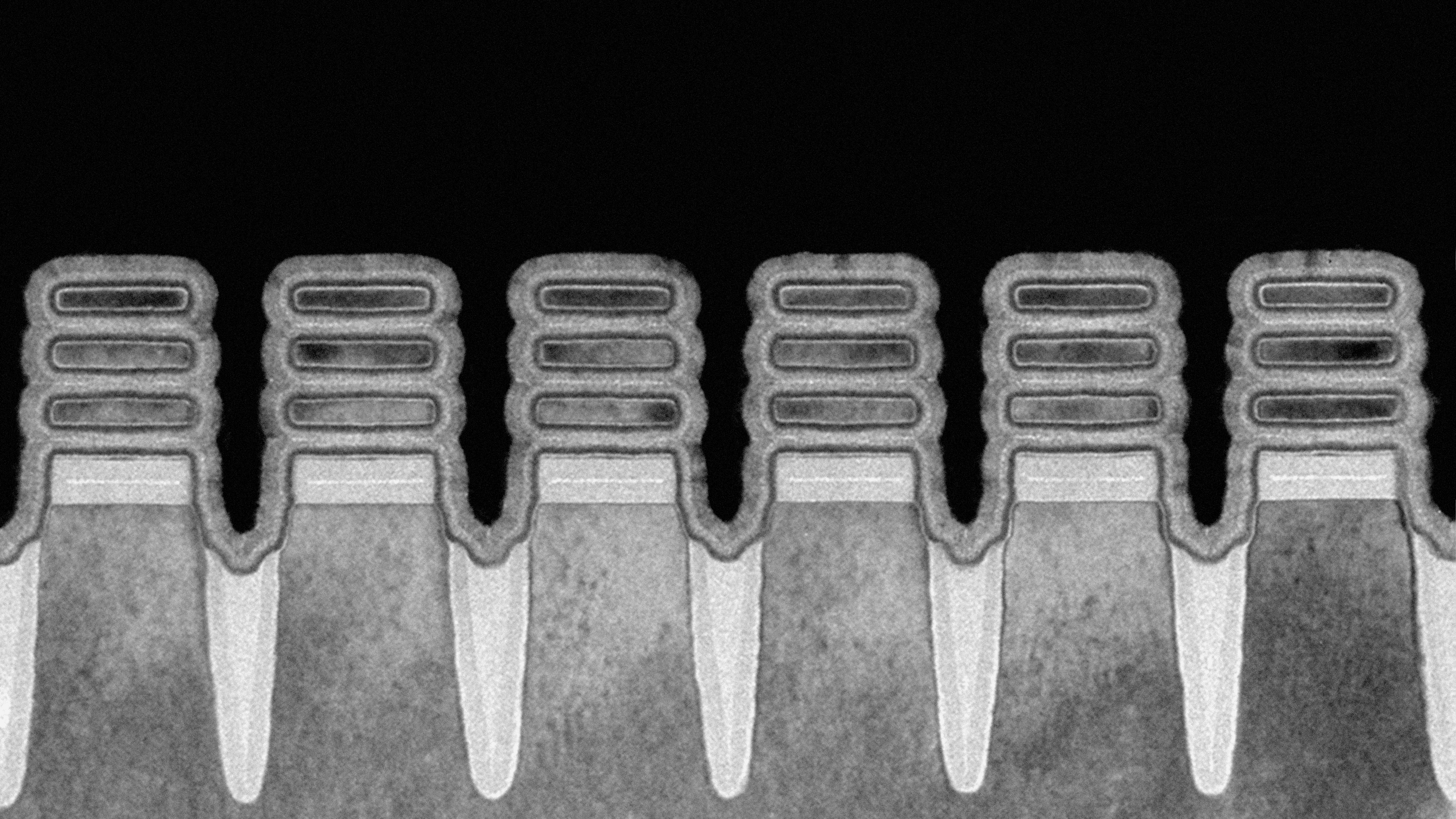
IBM circumvented this physical roadblock by deploying a pioneering Gate-All-Around (GAA) nanosheet architecture. In this design, the gate material completely surrounds the channel on all four sides, enabling superior electrostatic control. This technological leap allows current to flow freely through the nanosheets when the transistor is on, while effectively sealing off the channel to eliminate current leakage when the transistor is off.
The numbers emerging from the Albany labs are staggering:
- Transistor Density: 50 billion microscopic switches integrated onto a single die measuring roughly 150 square millimeters.
- Performance Differential: Up to a 45% increase in processing performance when operating at the same power level as current 7nm nodes.
- Power Efficiency: A monumental 75% reduction in power consumption for the same level of performance, allowing mobile devices to run for days without a charge and slashing cooling expenditures for hyper-scale cloud data centers.
In the context of enterprise IT infrastructure, these metrics translate directly into bottom-line savings. By lowering power draw, data center operators can mitigate escalating energy costs, optimize power usage effectiveness (PUE) ratings, and ease regulatory compliance burdens tied to carbon footprint reduction.
Verified Data & Metrics Breakdown

| Node Generation | Approximate Feature Size | Transistor Density / Count | Performance vs. Baseline (7nm) | Energy Efficiency Gains |
|---|---|---|---|---|
| 7nm Node (Baseline) | 7 Nanometers | Standard Commercial Density | Baseline (1x) | Baseline (1x) |
| 5nm Node | 5 Nanometers | High-Density Mobile SoCs | ~15% Faster | ~30% Less Power |
| IBM 2nm Test Chip | 2 Nanometers (GAA) | 50 Billion Transistors / Die | Up to 45% Faster | Up to 75% Less Power |
Industry & Market Implications: Capital Allocation and Geopolitical Resilience
The economic shockwaves of IBM’s breakthrough extend far beyond the laboratory. In the global semiconductor market, capital allocation is governed by extreme risk mitigation and astronomical R&D expenditures. Building a leading-edge fabrication facility now requires upwards of $20 billion in upfront capital investment, making technological milestones like IBM's 2nm chip critical validation points for future-proofing investments.
Who Wins:
- Enterprise Cloud Providers: Hyperscalers such as Amazon Web Services, Microsoft Azure, and Google Cloud stand to gain massive compute density and power savings, directly improving operating margins on heavy AI and machine learning workloads.
- Sovereign Technology Initiatives: By proving that advanced nodes can be successfully prototyped on U.S. soil, IBM reinforces national security objectives and mitigates single-region dependency risks.
- Foundry Partners: IBM’s legacy of licensing pioneering architectures (such as its historic collaboration model with Samsung and Intel) positions ecosystem partners to commercialize these blueprints for mass manufacturing.
Who Loses:
- Lagging Competitors: Foundries failing to successfully transition from FinFET to GAA architectures face immediate obsolescence in the high-performance computing (HPC) and premium mobile segments.
- Legacy Infrastructure Vendors: Data center hardware providers unable to integrate ultra-dense, low-power silicon risk losing market share as enterprises upgrade to power-optimized architectures.
From a macroeconomic perspective, the ability to squeeze 50 billion transistors into such a minute space alters market liquidity dynamics for venture capital and private equity firms eyeing deep tech. Investors are increasingly prioritizing hardware plays that solve fundamental thermodynamic constraints over purely software-driven efficiency gains.
People Also Ask (FAQ)
Frequently Asked Questions
What makes IBM’s 2nm chip different from current 7nm or 5nm commercial chips?
Unlike current commercial chips that rely on FinFET architecture, IBM’s 2nm chip utilizes a Gate-All-Around (GAA) nanosheet architecture. This design wraps the gate completely around the transistor channels, drastically reducing current leakage, boosting processing speeds by up to 45%, and cutting energy consumption by up to 75%.
When will IBM's 2nm technology be available in commercial devices and servers?
While IBM successfully demonstrated the functional prototype in May 2021 at its Albany Nanotech research facility, commercialization and mass manufacturing by foundry partners typically require a 3-to-4-year transition window, pointing toward widespread commercial adoption in the mid-2020s.
How does this breakthrough impact enterprise data center ROI and sustainability?
The 75% energy reduction directly addresses escalating data center electricity costs and cooling overhead. By packing 50 billion transistors into high-density architectures, enterprises can dramatically increase compute capacity without expanding physical data center footprints or exceeding local power grid limits.
Where was the 2nm test chip developed?
The chip was developed at IBM Research’s Albany Nanotech Complex located in New York State, serving as a primary hub for public-private semiconductor research and advanced prototyping in North America.
Future Outlook: Milestones on the Road to Mass Commercialization
As the semiconductor industry digests the implications of IBM’s milestone, attention now turns to the arduous execution phase of commercial scaling. Transitioning from a successful laboratory test chip at the Albany Nanotech Complex to high-volume manufacturing (HVM) requires solving complex lithography challenges, specifically mastering High-Numerical Aperture Extreme Ultraviolet (High-NA EUV) patterning tools.
Key milestones to watch over the next 24 to 36 months include:
- Foundry Yield Optimization: Scaling defect-free wafer yields from single-digit prototype runs to commercial-grade defect densities required for mass production.
- Ecosystem Tooling Integration: Adaptation of Electronic Design Automation (EDA) software suites to support GAA nanosheet layouts for fabless chip designers.
- Commercial Product Rollouts: Announcements from major fabrication partners and enterprise hardware vendors detailing enterprise server chips and mobile SoCs leveraging IBM-derived GAA IP.
Ultimately, IBM’s 2nm revelation proves that Moore’s Law is not dead—it is merely evolving. For enterprise leaders navigating digital transformation, artificial intelligence expansion, and rigorous ESG mandates, the arrival of 50-billion-transistor silicon provides the foundational hardware engine required to power the next decade of global economic growth.