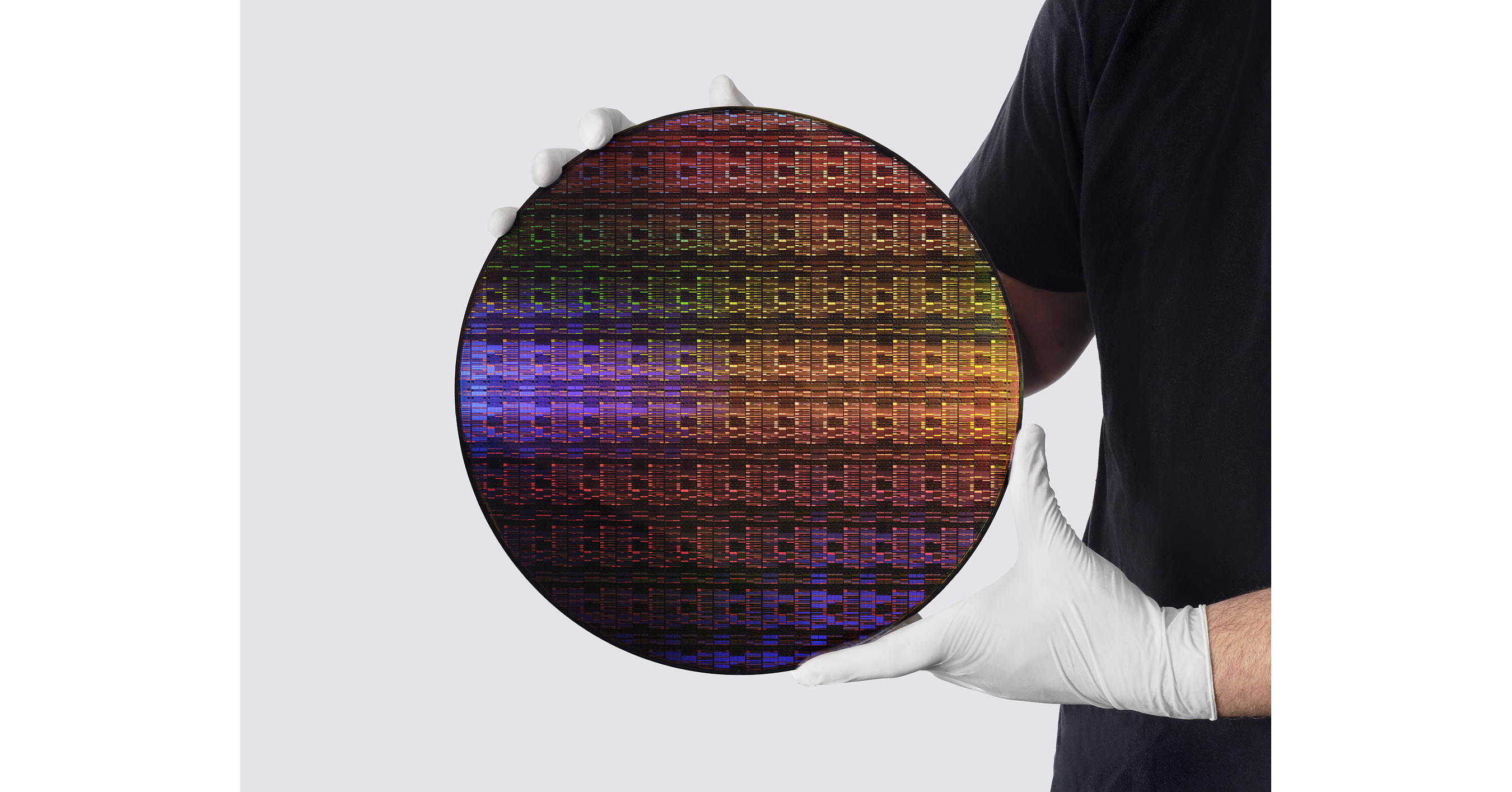
NEW YORK — In the high-stakes theater of semiconductor manufacturing, breakthroughs are measured not just in nanometers, but in the seismic shifts they trigger across global supply chains, capital expenditure cycles, and geopolitical balance sheets. On May 6, 2021, IBM Research detonated a technological shockwave across the enterprise computing landscape by unveiling the world’s first 2-nanometer (nm) node test chip. Packing an astonishing 50 billion transistors onto a piece of silicon roughly the size of a fingernail, this milestone at the Albany Nanotech Complex in New York did more than push the boundaries of physics—it redrew the roadmap for enterprise ROI, infrastructure scalability, and the future valuation multiples of the world’s most dominant technology conglomerates.
For institutional investors, corporate technologists, and macroeconomic strategists, the debut of IBM’s 2nm architecture arrived at a critical inflection point. As global chip shortages exposed the fragility of legacy supply chains and cloud hyperscalers strained against the power-consumption limits of existing infrastructure, the promise of a 45% performance boost or a 75% power reduction at the same operating voltage offered a compelling blueprint for next-generation risk mitigation and capital allocation.
Executive Takeaways
- Density Milestone: IBM Research successfully integrated 50 billion transistors onto a 2nm test chip, achieving a transistor density of 333 million transistors per square millimeter.
- Performance & Power Paradigm: The architecture delivers up to a 45% increase in computing performance or a 75% reduction in energy consumption compared to mainstream 7nm node chips currently powering millions of servers and devices.
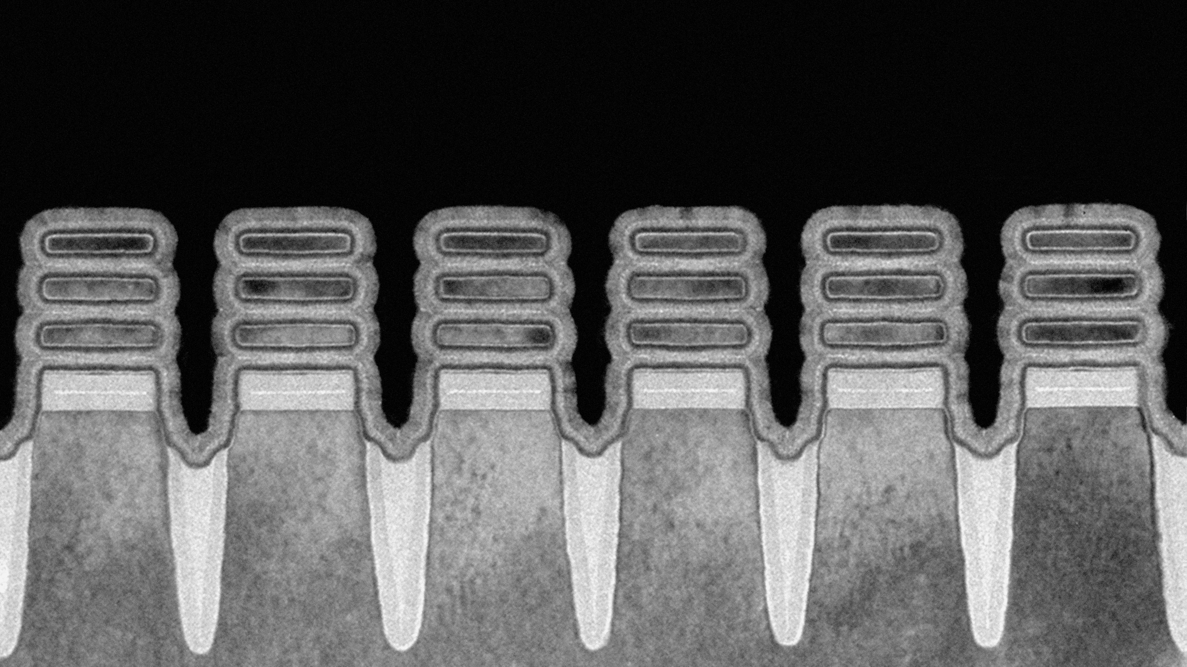
- Architectural Innovation: The breakthrough relies on a novel nanosheet (gate-all-around or GAA) transistor architecture, moving beyond traditional FinFET designs that have hit scaling walls below 5nm.
- Strategic Ecosystem Impact: By proving out the 2nm node, IBM strengthened its intellectual property portfolio and validated its joint-development manufacturing model with key industry partners like Samsung and Intel.
The Anatomy of a Breakthrough: Physics, Power, and the Nanosheet Architecture
Test Our Free AI & Tech Utilities Suite
Calculate LLM API token costs, analyze article dwell-time, or simulate tech DCA returns.
To understand the profound economic and technical implications of IBM’s May 2021 announcement, one must examine the fundamental laws of semiconductor physics that govern modern computing. For decades, Moore’s Law—the empirical observation that the number of transistors on a microchip doubles roughly every two years—has driven the exponential growth of enterprise software, cloud computing, and artificial intelligence. However, as lithography dipped below the 5nm threshold, traditional FinFET (Fin Field-Effect Transistor) architectures began running into severe quantum mechanical barriers. Current leakage, extreme thermal dissipation, and short-channel effects threatened to bring the silicon revolution to a grinding halt.
IBM’s research team, operating out of the Albany Nanotech Complex, bypassed these physical roadblocks by pioneering a vertically stacked nanosheet transistor architecture, often referred to in industry nomenclature as Gate-All-Around (GAA). Instead of the vertical fins of previous generations, IBM’s 2nm design utilizes horizontal sheets of silicon surrounded entirely by gate material. This multi-bridge channel architecture allows current to flow with far greater efficiency, exercising precise electrostatic control over the channel.
The resulting metrics are nothing short of revolutionary for cloud compute architecture and enterprise data centers:
- Die Scaling: Fitting 50 billion microscopic switches onto a footprint no larger than a fingernail allows for unprecedented functional integration, reducing signal latency between distinct logic blocks.
- Thermal Efficiency: By slashing power consumption by up to 75%, data center operators can dramatically lower cooling costs—a major operational expense that directly impacts enterprise EBITDA margins.
- Battery Longevity: For edge computing and mobile devices, a 75% power savings translates to smartphone batteries lasting up to four days on a single charge, while reducing the thermal throttling that plagues high-performance mobile applications.
This architectural leap also fundamentally alters the risk profile of high-density computing. As organizations migrate increasingly complex workloads—including large language models, real-time financial fraud detection algorithms, and high-frequency trading engines—the ability to compute more data per watt is no longer a luxury; it is a core regulatory compliance and cost-management imperative.
Verified Data & Metrics Breakdown

A rigorous comparative analysis of historical and emerging node technologies underscores the magnitude of IBM Research's 2021 milestone:
| Semiconductor Metric / Feature | Legacy 7nm Nodes | Advanced 5nm Nodes | IBM Research 2nm Test Chip |
|---|---|---|---|
| Approximate Transistor Count | ~10 Billion – 20 Billion | ~30 Billion – 40 Billion | 50 Billion |
| Transistor Architecture | FinFET | FinFET / Early GAA | Vertical Nanosheet (GAA) |
| Performance Gain vs. Baseline | Baseline Reference | ~15% – 20% Faster | Up to 45% Faster |
| Power Reduction at Same Speed | Baseline Reference | ~30% Lower Power | Up to 75% Lower Power |
| Primary Target Application | General Servers / Mobile | High-End Smartphones / GPUs | Cloud Hyperscalers, AI & High-Performance Computing (HPC) |
Industry & Market Implications: Capital Allocation and Geopolitical Realignment
The unveiling of the 2nm test chip reverberated far beyond academic laboratories, triggering immediate recalculations across global financial markets and corporate boardrooms. In the high-stakes ecosystem of semiconductor manufacturing, R&D breakthroughs dictate market liquidity, valuation multiples, and competitive dominance.
For enterprise buyers—ranging from major financial institutions running proprietary risk-modeling software to cloud giants like Amazon Web Services, Microsoft Azure, and Google Cloud—the availability of sub-3nm silicon promises a dramatic upgrade in infrastructure scalability. When compute density triples, the physical footprint of enterprise data centers shrinks, optimizing real estate capital expenditures and lowering energy infrastructure burdens.
However, the economic ripples are complex:
- The Capital Expenditure Hurdle: Transitioning a breakthrough from a research test chip to high-volume commercial manufacturing requires staggering capital allocation. Multi-billion-dollar investments in Extreme Ultraviolet (EUV) lithography equipment from suppliers like ASML are mandatory, creating high barriers to entry that favor only the most capitalized foundries.
- Ecosystem Partnerships: IBM’s historical strategy of developing foundational silicon technology and licensing or partnering for manufacturing—such as its alliances with Samsung and Intel—highlights a collaborative defense against pure-play monopoly risks in Asian foundries. This decentralization provides vital supply chain risk mitigation for Western economies.
- National Security & Sovereign Tech: With semiconductor supply chains treated as critical national security infrastructure, IBM’s success in New York reinforced domestic capabilities, aligning with federal initiatives like the U.S. CHIPS Act to onshore advanced manufacturing R&D.
Frequently Asked Questions (People Also Ask)
What exactly is a 2nm semiconductor chip, and how small is 2 nanometers?
A 2nm chip refers to a semiconductor manufacturing process node where critical features of the transistors—such as the gate length—are approximately 2 nanometers in size. For perspective, a strand of human hair is roughly 80,000 to 100,000 nanometers wide. At 2nm, features are so minute that quantum mechanical effects begin to take hold, requiring entirely new transistor designs like IBM’s nanosheet architecture to maintain electrical control.
Why is packing 50 billion transistors onto a fingernail-sized chip such a major milestone?
Transistors are the microscopic switches that process data. Packing 50 billion of them onto a silicon die roughly the size of a fingernail drastically shortens the electrical pathways between switches. This physical proximity reduces signal latency, increases raw processing speed, and allows chip designers to integrate more specialized processing units—such as AI accelerators and security coprocessors—onto a single piece of silicon.
How does IBM’s nanosheet (GAA) architecture differ from older FinFET designs?
Traditional FinFET transistors use vertical fins of silicon wrapped by a gate on three sides. As chips shrank below 5nm, controlling current leakage through three sides became increasingly difficult. IBM’s nanosheet architecture stacks horizontal ribbons of silicon, allowing the gate material to completely surround ("gate-all-around") every side of the channel. This provides superior electrostatic control, slashing power leakage and enabling the dramatic efficiency gains demonstrated in the 2nm test chip.
When will 2nm chips be commercially available in enterprise servers and consumer devices?
While IBM successfully demonstrated a functioning test chip in May 2021, moving from laboratory prototyping to high-volume manufacturing (HVM) is a multi-year engineering undertaking. Commercial foundries partnering with or licensing these technologies typically require two to four years to optimize yield rates, tooling, and mass production lines, putting widespread commercial deployment in the mid-2020s.
Future Outlook: The Road Ahead for Sub-Nanometer Silicon
As the semiconductor industry navigates the post-Moore’s Law era, innovations pioneered by institutions like IBM Research dictate the outer limits of human technological progress. The successful prototyping of the 2nm test chip proved that silicon scaling is far from dead; rather, it has entered a more sophisticated, architecturally diverse phase.
Over the next decade, key milestones to watch will include the successful yield optimization of gate-all-around nodes in commercial foundries, the integration of backside power delivery networks to further reduce resistive power loss, and the convergence of advanced packaging techniques like 3D chiplet integration. For enterprise leaders, maintaining a competitive advantage will require continuous monitoring of these hardware evolution cycles, ensuring that software architectures are optimized to exploit the unprecedented performance-per-watt efficiencies unlocked by sub-nanometer engineering.