Executive Takeaways
- Unprecedented Scale: IBM Research successfully prototyped the world’s first 2-nanometer (nm) node test chip, packing an astonishing 50 billion transistors onto a fingernail-sized die.
- Architectural Supremacy: The breakthrough relies on gate-all-around (GAA) nanosheet architecture, dramatically shifting capital allocation and design paradigms away from legacy FinFET limits.
- Commercial & Fiscal Impact: Promising a 45% performance boost or a 75% power reduction compared to standard 7nm nodes, this development directly reshapes enterprise ROI, hyperscale cloud compute architecture, and semiconductor valuation multiples.
- Geopolitical Stakes: As global supply chains face acute volatility, IBM’s milestone—born from its Albany, New York Nanotech Complex—underscores the critical nexus of sovereign risk mitigation, R&D tax incentives, and advanced manufacturing leadership.
ALBANY, N.Y. — In an industry where miniaturization dictates the bounds of human capability, the laws of physics have long threatened to halt the relentless cadence of Moore’s Law. On May 6, 2021, Big Blue decisively altered that narrative. IBM Research formally announced the successful fabrication of the world’s first 2-nanometer (nm) test chip at its Albany Nanotech Complex, integrating an unprecedented 50 billion transistors onto a sliver of silicon no larger than a fingernail.
For institutional investors, enterprise IT architects, and sovereign regulators, this announcement was far more than an academic milestone. It represented a structural pivot point in global technology infrastructure. By achieving densities that translate to roughly 333 million transistors per square millimeter, IBM demonstrated that the path to next-generation computing efficiency—critical for data-intensive workloads like artificial intelligence, 5G/6G cellular routing, and autonomous systems—remains wide open.
The Physics of the Microscopic: Anatomy of a 2nm Breakthrough
Test Our Free AI & Tech Utilities Suite
Calculate LLM API token costs, analyze article dwell-time, or simulate tech DCA returns.
To contextualize the magnitude of IBM’s May 2021 disclosure, one must examine the severe physical bottlenecks facing modern semiconductor manufacturing. As nodes shrink below the 5nm and 3nm thresholds, traditional FinFET (Fin Field-Effect Transistor) architectures begin to suffer from severe current leakage and short-channel effects. Controlling electron flow through a channel becomes exceptionally difficult when the dimensions approach the scale of individual atoms.
IBM’s research team bypassed this physical wall by pioneering a gate-all-around (GAA) nanosheet transistor architecture. Instead of the vertical fins characteristic of FinFETs, IBM utilized stacked silicon nanosheets that allow the gate material to wrap completely around the channel. This multi-gate design maximizes electrostatic control, virtually eliminating leakage current and enabling hyper-precise switching states.
- Dimensional Mastery: The nanosheets can be adjusted in width—ranging from 15 to 70 nanometers—giving chip architects unprecedented flexibility to balance power and performance requirements on a single monolithic die.
- Density Milestone: Fitting 50 billion microscopic switches into a sub-150-square-millimeter footprint required extreme ultraviolet (EUV) lithography optimizations, pushing multi-patterning techniques to their absolute limits.
- Voltage Efficiency: Operating at lower voltages without sacrificing switching speed, the architecture directly addresses the thermal dissipation crises plaguing hyperscale data centers and edge-computing deployments alike.
Darrell Hill, then vice president of research at IBM, noted during the initial briefings that the leap to 2nm was not merely incremental, but a foundational redesign of how semiconductor physics interact with enterprise compute demands. The engineering triumph required years of material science breakthroughs, specifically involving novel high-k metal gate (HKMG) stacks and inner-spacer dielectric films capable of withstanding extreme thermal budgets during fabrication.
Verified Data & Metrics Breakdown Table
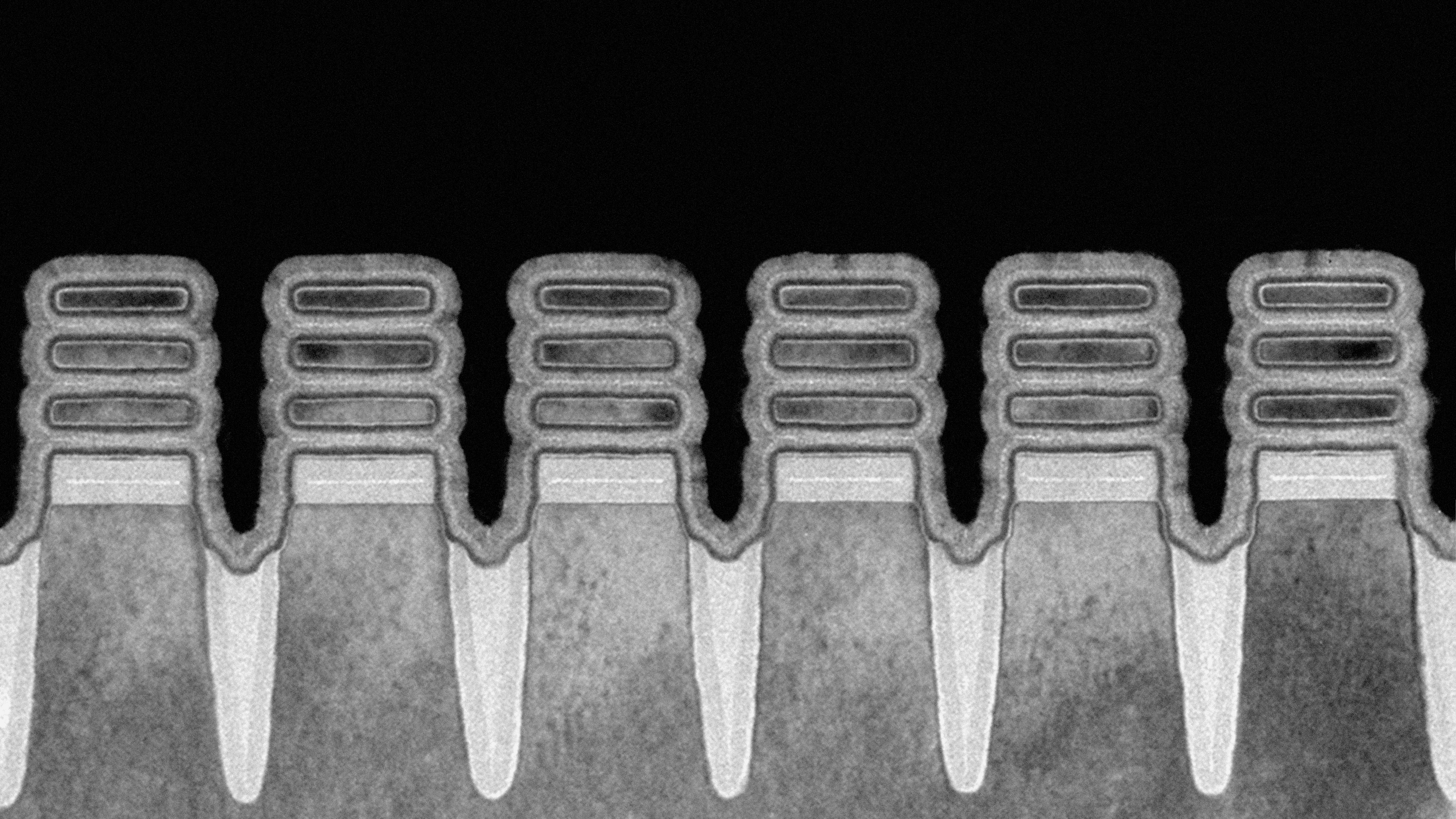
To evaluate the real-world operational impact of IBM’s 2nm test chip, industry analysts benchmarked its projected performance against prevailing commercial standards of the era. The following metrics illustrate the comparative advantages of the 2nm GAA architecture:
| Metric / Parameter | Standard 7nm Node (Baseline) | IBM 2nm Test Chip (Projected) | Comparative Delta / Advantage |
|---|---|---|---|
| Transistor Density | ~90–100M transistors / mm² | ~333M transistors / mm² | >3x Density Increase |
| Performance Gain (at equal power) | Baseline (1.0x) | +45% Speed Increase | Significant reduction in processing bottlenecks |
| Power Reduction (at equal performance) | Baseline (1.0x) | -75% Energy Consumption | Massive operational expenditure (OpEx) savings |
| Battery Life Impact (Mobile Devices) | Standard Daily Cycle | Up to 4x Quadrupled Battery Life | Transforms mobile form-factor longevity |
| Primary Architecture | FinFET (Fin Field-Effect Transistor) | GAA Nanosheet (Gate-All-Around) | Eliminates short-channel current leakage |
Industry & Market Implications: Winners, Losers, and Economic Shifts
The unveiling of the 2nm milestone sent immediate shockwaves across the global semiconductor ecosystem, influencing capital allocation strategies from Wall Street to Taipei. In an industry where capital expenditure (CapEx) for fabrication plants (fabs) routinely exceeds $20 billion per facility, technological leadership translates directly into pricing power and high gross margins.
Enterprise ROI and Cloud Infrastructure Scalability
For enterprise CIOs and hyperscale cloud providers—including Amazon Web Services, Microsoft Azure, and Google Cloud—the arrival of 2nm technology promises a radical reimagining of server hardware efficiency. Data center power consumption has emerged as a primary constraint on enterprise growth, with cooling and electricity costs threatening corporate sustainability mandates and profit margins. A 75% reduction in power consumption at equivalent performance levels allows data center operators to quadruple rack densities without triggering thermal overloads or necessitating costly grid infrastructure upgrades. This translates directly into superior enterprise ROI and lower total cost of ownership (TCO).
Supply Chain Dynamics and Geopolitical Risk Mitigation
Geopolitically, IBM’s announcement reinforced the strategic importance of domestic semiconductor R&D. Developed within a public-private research ecosystem in Upstate New York—featuring partnerships with organizations like NY CREATES and global foundries—the breakthrough highlighted the efficacy of targeted government investment. As policymakers in Washington and Brussels wrangled over legislation like the U.S. CHIPS Act, IBM’s 2nm reveal provided empirical proof that Western institutions retained the intellectual property and scientific talent required to lead the next generation of hardware engineering.
Competitive Pressures on Foundry Giants
While IBM operates primarily as a research and systems enterprise rather than a high-volume foundry (having previously spun off its manufacturing operations to GlobalFoundries and licensing its node designs to partners like Samsung and Intel), the 2nm test chip set the benchmark for commercial foundries. Companies like TSMC, Samsung Electronics, and Intel found their roadmap validation accelerated, as enterprise customers began demanding similar GAA nanosheet guarantees for their upcoming product generations.
Frequently Asked Questions (People Also Ask)
What is a 2nm chip, and why is IBM’s 50-billion transistor milestone significant?
A 2nm chip refers to a semiconductor manufactured using a process node where individual transistor features measure approximately 2 nanometers—roughly the size of a strand of DNA. IBM’s milestone of packing 50 billion of these microscopic switches onto a fingernail-sized die is significant because it dramatically increases processing power while curbing power consumption, overcoming the physical leakage barriers that rendered older FinFET architectures obsolete at sub-3nm scales.
How does Gate-All-Around (GAA) nanosheet architecture work?
Unlike traditional FinFET transistors where the conductive channel is gripped by the gate on three sides, GAA nanosheet architecture wraps the gate material entirely around horizontal silicon channels (nanosheets). This complete enclosure provides superior electrostatic control over electron flow, drastically reducing current leakage and allowing electrons to travel more efficiently through the circuit.
What are the primary real-world benefits for enterprise and consumer technology?
According to IBM’s benchmark data, the 2nm architecture delivers either a 45% increase in processing performance or a 75% reduction in power consumption compared to standard 7nm chips. For consumers, this translates to smartphone battery life that could last up to four days between charges. For enterprises, it enables hyper-efficient hyperscale cloud computing, faster artificial intelligence training models, and reduced cooling requirements in data centers.
When did commercial devices utilizing 2nm technology become available?
Following IBM’s initial test chip unveiling in May 2021, commercial foundry implementation required several years of tooling, yield optimization, and ecosystem alignment. Major semiconductor foundries began high-volume commercial production of 2nm-class nodes targeting consumer devices and enterprise server processors in the 2024 to 2026 timeframe.
Future Outlook: The Road Beyond 2nm and What to Watch
As the semiconductor industry transitions from experimental test chips to mass-market commercialization, the strategic focus shifts toward the next operational horizons. The success of IBM’s 2nm test chip proved that lithographic scaling remains viable, but it also exposed the escalating complexity of packaging, thermal management, and lithographic alignment.
Key milestones and indicators to monitor across the macroeconomic and technological landscape include:
- High-NA EUV Adoption: The integration of High Numerical Aperture Extreme Ultraviolet lithography systems by leading foundries to pattern sub-2nm features with fewer exposure steps, directly influencing manufacturing yields and wafer costs.
- Advanced Packaging & Chiplet Integration: Moving beyond monolithic dies, the combination of 2nm compute tiles with high-bandwidth memory (HBM) and I/O dies via 3D packaging technologies (such as backside power delivery networks) to maximize enterprise compute density.
- Regulatory and Subsidy Execution: The tangible output of global government funding initiatives—such as the U.S. CHIPS and Science Act and European Chips Act—in establishing secure, domestic advanced packaging and fabrication facilities capable of supporting next-generation nodes.
- Sustaining Margin Health: How semiconductor designers and foundries pass on the escalating R&D and tooling costs of sub-2nm nodes to enterprise buyers without compressing enterprise adoption velocity.
Ultimately, IBM’s 2nm breakthrough served as a vital psychological and technical watershed. By demonstrating that the physical limits of silicon could be engineered around through innovative nanosheet geometry, the industry secured its trajectory for the remainder of the decade—redefining the contours of enterprise performance, national security, and digital infrastructure for years to come.