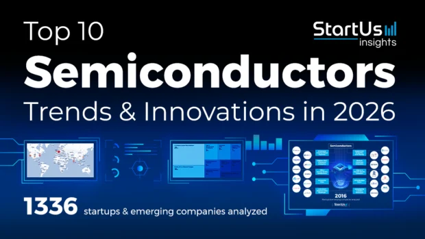
WASHINGTON, LONDON, TOKYO — Feb 24, 2026 — Data released today by market intelligence firm StartUs Insights, coupled with global channel checks across Silicon Valley, Hsinchu, and Eindhoven, confirms a critical economic threshold: the semiconductor industry has officially entered the $1 trillion valuation era. Driven by insatiable enterprise appetite for generative AI models, autonomous computing engines, and hyperscale cloud infrastructure, the chip sector is undergoing its most radical structural evolution in half a century. The traditional playbook of monolithic silicon scaling has broken down, giving way to advanced heterogeneous integration, sub-2nm transistor topologies, and domain-specific co-processors.
As corporate capital expenditure allocations shift heavily toward enterprise infrastructure scalability, semiconductor capital intensity has reached unprecedented levels. Tier-1 fabricators, cloud hyperscalers, and fabless designers are making tens of billions in capital commitments to master ten distinct technology vectors. This investigative report analyzes the architectural shifts, financial dynamics, and geopolitical forces dictating the semiconductor supply chain in 2026.
Executive Takeaways
- The $1 Trillion Capital Paradigm: Global semiconductor revenues are crossing $1 trillion in 2026, catalyzed by hyperscale AI infrastructure deployments, custom enterprise silicon, and automotive electrification.
- Sub-2nm GAA and Advanced Substrates: Commercial production at sub-2nm nodes using Gate-All-Around (GAA) nanosheets, alongside the deployment of glass substrates, is replacing legacy FinFET architectures to overcome physical scaling limits.
- Hyperscaler ASIC Disruption: Big Tech capital expenditure is pivoting toward custom Application-Specific Integrated Circuits (ASICs), directly challenging legacy merchant GPU gross margin structures and reshaping chip designer enterprise valuations.
- Supply Chain Regionalization: Multibillion-dollar government subsidies from the US CHIPS Act and European Chips Act are bringing physical manufacturing online, fundamentally shifting global fab utilization rates and risk mitigation models.
The Anatomy of the Silicon Transformation: 10 Mega-Trends in 2026

1. Sub-2nm Gate-All-Around (GAA) Transistor Dominance
As FinFET technology encounters insurmountable physical leakage limits at lower geometries, the industry has universally pivoted to Gate-All-Around (GAA) nanosheet architectures. In 2026, TSMC's N2 process, Samsung's SF2, and Intel's 18A nodes are operating at commercial scale. GAA enables finer electrostatic control, allowing chip designers to squeeze up to 30% higher power efficiency and 15% greater clock frequency out of identical power envelopes—crucial parameters for heat-constrained hyperscale data centers.
2. Advanced Packaging and Glass Substrate Adoption
Monolithic die scaling has hit an economic wall; yielding a massive 800mm² die on sub-2nm nodes is cost-prohibitive. Consequently, advanced packaging technologies—such as TSMC's CoWoS-S/L, Intel's Foveros Direct, and 3D chiplet integration—have become the primary vector for density gains. Furthermore, 2026 marks the first wave of commercial deployment for glass substrates. Replacing organic materials, glass provides superior mechanical flatness, structural integrity, and thermal tolerance, allowing for massive interposer sizes and high-density optical interconnects.
3. High-Bandwidth Memory (HBM4) and Optical Compute Interconnects
Memory bandwidth bottlenecks remain the chief obstacle to scaling ultra-large AI models. The industry transition to HBM4 in 2026 introduces a 2048-bit bus interface, doubling the interconnect density compared to HBM3e. To bypass copper's physical latency and power penalties across large data center clusters, silicon photonics—specifically Co-Packaged Optics (CPO)—is being integrated directly onto the chiplet package, transmitting data using light across fiber arrays.
4. The Proliferation of Custom Hyperscaler Silicon
To preserve operating margins and mitigate vendor lock-in, tier-1 cloud providers (AWS, Google, Meta, and Microsoft) are channeling capital allocation toward in-house custom ASICs. Proprietary accelerators tailored specifically for inference workloads are systematically undercutting monolithic merchant GPUs on a performance-per-watt and total cost of ownership (TCO) basis, altering long-term enterprise software unit economics.
5. Compound Semiconductors (GaN & SiC) in Data Center Power Trains
Data center power delivery has emerged as an urgent operational bottleneck. The adoption of wide-bandgap compound semiconductors—Gallium Nitride (GaN) and Silicon Carbide (SiC)—has expanded beyond electric vehicle powertrains directly into hyperscale power distribution units (PDUs). 2026 saw the conversion of rack-level power architectures from 12V to 48V, utilizing GaN and SiC power switches to achieve 98%+ power conversion efficiency and drastically shrink footprint requirements.
6. Generative AI-Driven Electronic Design Automation (EDA)
Designing modern chips featuring over 100 billion transistors is humanly unmanageable without autonomous tooling. Leading EDA providers (Synopsys, Cadence) have fully embedded generative AI agents into physical layout design, floorplanning, and timing closure workflows. In 2026, AI-driven EDA tools have cut tape-out schedules by up to 40%, optimizing floorplans for thermal dissipation and yield-curve optimization prior to physical silicon manufacturing.
7. Edge Neuromorphic and In-Memory Computing
Running multi-billion parameter AI models at the edge—in smart appliances, industrial robotics, and personal mobility devices—requires micro-watt power consumption. Neuromorphic microprocessors that mimic biological brain spikes, alongside Analog In-Memory Computing (AIMC) architectures that perform matrix multiplication directly within non-volatile flash or Resistive RAM (ReRAM) cell arrays, are eliminating the high-power memory fetch cycle entirely.
8. Geopolitical Supply Chain Localization & Fab Maturity
The geopolitical mandate for supply chain redundancy has reached operational maturity. Multi-billion dollar sovereign facilities funded under the US CHIPS Act, European Chips Act, and Japanese subsidies are officially printing commercial wafers in 2026. While this geographic distribution mitigates single-point-of-failure geopolitical risks in East Asia, it introduces macro margin pressure as operational expenses and labor cost differentials digest fab depreciation schedules across Western regions.
9. Quantum-Silicon Cryogenic Interfaces
As quantum computing moves out of experimental laboratories and into practical hybrid computing configurations, silicon microelectronics have adapted to serve cryogenic control systems. In 2026, highly specialized silicon-germanium (SiGe) control chips operating at liquid-helium temperatures (4 Kelvin and below) are mounted directly adjacent to quantum processing units (QPUs), replacing thousands of bulky coaxial cables with high-speed serialized silicon buses.
10. On-Chip Hardware-Enforced Zero-Trust Security
With generative AI enabling unprecedented cyber threats, hardware-level security is non-negotiable. 2026 enterprise microarchitectures feature dedicated, physically isolated security engines equipped with hardcoded Post-Quantum Cryptography (PQC) primitives. Silicon Root-of-Trust (RoT) chips now monitor bus traffic in real time via continuous side-channel attack inspection engines, isolating compromised memory blocks at the hardware level before malware can exploit the hypervisor.
Data & Metrics Breakdown: Semiconductor Shift in 2026
| Technology Vector | Dominant 2026 Standard | Key Performance / Efficiency Metric | Primary Enterprise Drivers |
|---|---|---|---|
| Transistor Architecture | Sub-2nm Gate-All-Around (GAA) | 15% Clock Speed / 30% Power Reduction | Data Center & Hyperscale Compute |
| Advanced Packaging | Glass Substrates & 3D Wafer Bonding | >10x Interconnect Density vs. Organic | AI Accelerators & HPC Chiplets |
| Memory Architecture | HBM4 (2048-bit Bus Width) | 2.0+ TB/s Bandwidth per Stack | LLM Training & Inference Clusters |
| Optical Interconnects | Co-Packaged Optics (CPO) | 50% Power Reduction in Inter-Rack Data Movement | Hyperscale Networking Fabrics |
| Power Electronics | GaN / SiC 48V Rack Architectures | 98.5% Power Conversion Efficiency | Hyperscale PDU Thermal Management |
Industry & Market Implications: Capital Allocation & Structural Winners
The shift toward custom domain-specific hardware and sub-2nm architectures is driving massive realignments across equity markets and corporate debt structures. Pure-play foundries capable of supporting sub-2nm production and advanced 3D packaging are commanding historical valuation multiples, enjoying significant pricing power over fabless customers competing for wafer allocations.
Conversely, secondary market players that fail to master advanced heterogeneous packaging risk margin compression. As Big Tech hyperscalers substitute standard off-the-shelf accelerators with internal custom silicon designs, legacy chip designers must defend their total addressable market (TAM) by bundling software ecosystems deeply into hardware stacks. Meanwhile, Specialized Equipment Manufacturers (SEMs) offering High-NA EUV lithography tools, atomic layer deposition (ALD) systems, and advanced packaging test capabilities maintain high earnings quality and pricing power, serving as critical bottlenecks to the entire trillion-dollar engine.
Frequently Asked Questions (People Also Ask)
What is driving the global semiconductor industry toward a $1 trillion market size in 2026?
The primary driver is the infrastructure buildout for Artificial Intelligence, advanced edge computing, and cloud infrastructure. Generative AI requires exponential scaling in compute density, High-Bandwidth Memory (HBM4), and specialized power delivery chips. Additionally, the electrification of the automotive sector and the industrial Internet of Things (IoT) have significantly expanded silicon content per end product, driving long-term volume demand across advanced and mature nodes.
How does Gate-All-Around (GAA) technology differ from older FinFET transistor designs?
FinFET architectures feature a gate that covers a conducting channel on three sides. At nodes below 3nm, leakage currents increase significantly due to quantum tunneling effects. Gate-All-Around (GAA) technology wraps the gate material entirely around horizontal nanosheet channels on all four sides. This structural change optimizes electrostatic control, allows higher current density, minimizes dynamic power leakage, and enables higher operational clock speeds within a tighter thermal envelope.
Why are glass substrates being adopted in advanced semiconductor packaging?
Traditional organic substrates suffer from physical warpage, limited thermal tolerance, and low interconnect density limits under heavy multi-chiplet processing loads. Glass substrates offer exceptional dimensional stability, high flatness, superior thermal properties, and reduced signal loss. This allows chip designers to build larger optical-electrical interposers, integrate high-density optical connections, and combine dozens of compute and memory chiplets onto a single structural base without structural degradation.
Are custom enterprise ASICs replacing traditional merchant GPUs in 2026?
While merchant GPUs remain dominant for initial model training due to their versatile software ecosystems, custom enterprise Application-Specific Integrated Circuits (ASICs) are taking significant market share in inference workloads. Cloud hyperscalers are deploying custom ASICs to drastically lower energy costs per query, improve supply chain predictability, and reduce software latency, driving down overall enterprise infrastructure spending.
Future Outlook: Strategic Horizon Beyond 2026
As the semiconductor industry cements its position as the baseline utility of the global economy, attention is shifting toward the next horizon: full optical computing matrices, High-Numerical Aperture (High-NA) EUV manufacturing maturity, and atomic-scale 2D materials like transition metal dichalcogenides (TMCs). Institutional investors and enterprise procurement directors must maintain balanced capital strategies, taking into account fab construction timelines, geopolitical risk mitigation, and technological shifts across the hardware-software stack.
Organizations that successfully integrate custom silicon strategies, secure reliable packaging capacity, and adopt energy-efficient compute topologies will achieve substantial competitive moats in the trillion-dollar intelligence economy.