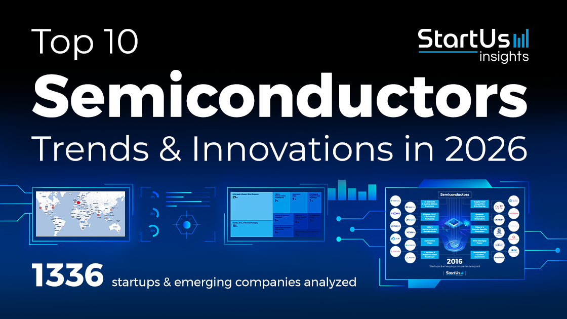
WASHINGTON, LONDON, TOKYO — As global capital expenditure targeting artificial intelligence infrastructure breaches historic thresholds, the semiconductor industry has crossed a definitive Rubicon. Valuations across the ecosystem no longer hinge merely on cyclical consumer electronics demand, but on the relentless, structurally driven expansion of enterprise-scale accelerated computing. According to comprehensive intelligence data released by StartUs Insights on February 24, 2026, the global hardware stack is undergoing a profound structural metamorphosis, characterized by the convergence of customer-defined microarchitectures, heterogeneous 3D integration, and unprecedented energy-density constraints.
For institutional investors, enterprise risk officers, and cloud compute architects, navigating this paradigm requires acute visibility into how underlying manufacturing, packaging, and design trends will dictate market liquidity and valuation multiples over the next decade. Below is our exhaustive investigative report detailing the ten transformative semiconductor trends steering the trillion-dollar AI and advanced computing economy in 2026.
Executive Takeaways
- Customer-Defined Silicon: Hyperscalers and mega-cap enterprises are abandoning off-the-shelf accelerators in favor of proprietary, application-specific integrated circuits (ASICs) tailored to proprietary model architectures.
- Thermal and Power Wall Realities: With generative AI data centers routinely pushing multi-megawatt thresholds, liquid cooling, advanced backside power delivery networks (BSPDN), and energy-efficiency metrics have become the primary determinants of infrastructure scalability and enterprise ROI.
- Advanced Packaging Hegemony: Monolithic die scaling has hit fundamental economic and physical limits; hybrid bonding, chiplet ecosystems, and 2.5D/3D integration now dictate time-to-market and manufacturing yield.
- Geopolitical Supply Chain Realignment: Capital allocation strategies are increasingly governed by regulatory compliance, onshoring mandates, and the imperative for supply chain risk mitigation across North America, Europe, and East Asia.
The Structural Catalyst: Why 2026 Marks a Watershed Moment
The macroeconomic backdrop of 2026 is defined by a singular economic reality: generative AI has transitioned from an exploratory enterprise experiment to the core operating layer of global commerce. Consequently, enterprise infrastructure scalability is inextricably linked to silicon throughput. As model parameter counts soar past the multi-trillion mark, traditional von Neumann computing architectures face crippling memory bandwidth bottlenecks and insurmountable thermal dissipation barriers.
The StartUs Insights findings underscore that survival in the modern compute economy demands more than incremental transistor shrinkage under Moore’s Law. Instead, the industry is relying on radical architectural departures. Semiconductor firms that successfully harmonize design flexibility with ultra-dense packaging are commanding premium market capitalizations, while legacy manufacturers slow to pivot face severe valuation compression.
The Top 10 Semiconductor Trends Powering the Advanced Computing Era
1. Customer-Defined and Hyperscale-Specific Silicon
The era of relying solely on general-purpose GPUs is maturing. In 2026, the world’s largest cloud service providers—spanning AWS, Microsoft Azure, Google Cloud, and Meta—are aggressively deploying customer-defined ASICs. By co-designing hardware specifically tailored to their proprietary large language model (LLM) training and inference workloads, these enterprises bypass third-party margins, optimize latency, and achieve vastly superior performance-per-watt ratios.
2. Advanced 3D Packaging and Chiplet Heterogeneity
As lithography costs at sub-2nm nodes skyrocket, the industry has universally embraced modular chiplet architectures. By breaking monolithic processors into smaller, specialized functional blocks (compute tiles, memory controllers, I/O interfaces) and interconnecting them via advanced 2.5D and 3D packaging technologies like TSMC’s CoWoS and Intel’s EMIB, manufacturers drastically improve yields and accelerate time-to-market.
3. Backside Power Delivery Networks (BSPDN)
Power routing has emerged as the single most critical electrical engineering bottleneck in advanced node manufacturing. By moving power delivery networks from the front side of the silicon wafer to the backside—exemplified by Intel’s PowerVia and TSMC’s similar nano-TSV implementations—engineers eliminate resistive voltage droop, drastically reduce signal interference, and reclaim precious routing real estate for high-density logic.
4. Photonics and Silicon Photonics Integration
Electrical copper interconnects within data centers are rapidly approaching physical bandwidth and thermal limits. The integration of optical transceivers directly onto silicon substrates—silicon photonics—allows data centers to transmit massive volumes of data between server racks using light rather than electrons. This trend is vital for mitigating network latency in distributed multi-node AI clusters.
5. Extreme Ultraviolet (EUV) and High-NA EUV Manufacturing
Lithography leadership remains the ultimate economic moat in the semiconductor supply chain. The commercialization and scaling of High-Numerical Aperture (High-NA) EUV systems throughout 2026 allow foundries to print even finer features without multi-patterning complexity. This capability directly enables the production of sub-2nm gate-all-around (GAA) transistors required for next-generation AI accelerators.
6. Liquid Cooling and Advanced Thermal Management Infrastructure
Semiconductor power densities have rendered traditional air cooling obsolete. High-performance compute nodes operating at hundreds of watts per socket necessitate direct-to-chip liquid cooling loops and immersion cooling systems. Enterprise capital expenditure allocations now routinely bundle advanced thermal management infrastructure directly into facility design, prioritizing power usage effectiveness (PUE) metrics.
7. Compute-in-Memory (CiM) and Processing-in-Memory (PiM)
The perennial "memory wall"—the latency and energy penalty incurred when shuttling data back and forth between separate logic and DRAM chips—is being dismantled by Compute-in-Memory architectures. By embedding processing elements directly inside memory arrays, CiM drastically accelerates inference tasks, reducing energy consumption by orders of magnitude for edge and data center AI workloads alike.
8. Automated Design Verification and AI-Driven EDA
Electronic Design Automation (EDA) has undergone an AI revolution. Modern chip complexity far exceeds human verification capabilities, forcing design houses to deploy machine learning algorithms to automate floorplanning, timing closure, and bug detection. AI-driven EDA tools shorten design cycles from years to months, allowing firms to iterate rapidly in response to shifting market demands.
9. Edge AI Microcontrollers and Neuromorphic Architectures
While hyper-scale data centers grab headlines, the proliferation of real-time AI at the network edge requires ultra-low-power silicon. Neuromorphic chips—which mimic the event-driven, spiking neural networks of the biological brain—are gaining commercial traction in autonomous systems, IoT devices, and robotics, enabling real-time decision-making with minimal power footprints.
10. Geopolitical Supply Chain Diversification and Resilience
Mitigating geopolitical risk is no longer a secondary boardroom concern; it is a board-level imperative governing capital allocation. Driven by legislative catalysts like the U.S. CHIPS Act and European equivalents, foundries and OSATs (Outsourced Semiconductor Assembly and Test) are aggressively diversifying geographic footprints. Building localized, resilient manufacturing ecosystems across North America, Europe, and allied Asian nations ensures regulatory compliance and protects against regional disruptions.
Verified Data & Metrics Breakdown
To quantify the velocity of this technological shift, the following comparative matrix details the key technical, financial, and operational benchmarks defining the 2026 semiconductor landscape:
| Technology / Trend Dimension | Legacy Benchmark (Pre-2024) | 2026 Current Standard | Primary Economic / Operational Impact |
|---|---|---|---|
| Node Architecture | FinFET (3nm / 5nm) | GAAFET & Early High-NA EUV Production | Improved transistor control, lower leakage, higher density. |
| Power Delivery | Front-Side Power Routing | Backside Power Delivery (BSPDN) | Eliminates voltage drop; boosts performance by 15-20%. |
| Packaging Paradigm | Monolithic Dies & Standard Wire-Bonding | Hybrid Bonding & Multi-Chiplet 3D Stacks | Higher manufacturing yields; circumvents reticle size limits. |
| Data Center Cooling | Air-Cooled Server Racks | Direct-to-Chip Liquid & Immersion Cooling | Enables multi-megawatt rack densities without thermal throttling. |
| Interconnect Technology | Copper Electrical Traces | Silicon Photonics & Optical IO | Overcomes copper bandwidth caps; drastically reduces latency. |
Industry & Market Implications: Winners, Losers, and Economic Realities
The trillion-dollar capital allocation wave currently sweeping the semiconductor sector is redrawing the competitive map. Financial markets are aggressively rewarding vertical integration and process leadership.
Who Wins
- Pure-Play Advanced Foundries & Equipment Makers: Companies mastering High-NA EUV lithography, deposition tools, and advanced packaging foundries (such as TSMC, ASML, and key equipment suppliers) are securing robust pricing power and high operating margins.
- Hyperscale ASIC Developers: Cloud titans successfully deploying proprietary custom silicon are insulating themselves from hardware commoditization, optimizing operating costs while delivering superior AI performance to enterprise clients.
- Thermal and Power Management Specialists: Firms providing liquid cooling loops, advanced power modules, and electrical grid interface hardware are experiencing unprecedented demand surges as data center power requirements outstrip local grid capacities.
Who Loses
- Legacy Semiconductor Manufacturers: Fabless and IDM firms slow to adopt chiplet methodologies or wedded exclusively to older planar or early FinFET nodes face severe margin erosion and declining market share.
- Commodity Memory Vendors Lacking HBM Capacity: Suppliers dependent entirely on standard consumer DRAM and NAND flash without robust High Bandwidth Memory (HBM) pipelines are missing out on the high-margin AI compute windfall.
Frequently Asked Questions (People Also Ask)
What drives the shift toward customer-defined silicon in 2026?
The shift is driven by the economic necessity for hyperscalers and major enterprises to optimize performance-per-watt and lower total cost of ownership (TCO) for specific AI workloads. Standard off-the-shelf GPUs, while versatile, introduce architectural overhead and third-party markup. Custom ASICs allow organizations to fine-tune silicon directly to their proprietary algorithmic structures, maximizing computational throughput.
How does backside power delivery (BSPDN) improve semiconductor performance?
BSPDN decouples power routing from signal routing by moving power delivery to the underside of the silicon wafer. This eliminates resistive voltage drops that plague traditional front-side networks, reduces signal crosstalk, and allows transistor densities to scale further without suffering severe thermal or electrical degradation.
Why is advanced packaging becoming more important than monolithic die scaling?
Monolithic die scaling has hit severe economic and physical walls; as chips grow larger, manufacturing defect rates spike and costs become prohibitive due to reticle size limits. Advanced packaging—such as 2.5D/3D chiplet integration—allows manufacturers to combine smaller, high-yield functional dies using ultra-dense interconnects, achieving greater overall performance at a fraction of the cost.
What role does silicon photonics play in modern AI data centers?
Silicon photonics replaces traditional copper electrical interconnects with optical connections, using light to transmit data between server nodes and racks. This eliminates bandwidth bottlenecks and latency constraints inherent in copper cabling, enabling the seamless scaling of massive, multi-node AI training clusters.
Future Outlook: What Comes Next
Looking past 2026, the trajectory of the semiconductor industry will be dictated by the commercialization of sub-1nm gate architectures, atomic-level precision manufacturing, and the eventual integration of quantum-accelerated coprocessors into standard data center fabrics. As enterprise ROI scrutiny intensifies, semiconductor innovation will no longer be judged solely by raw clock speeds or transistor counts, but by systemic energy efficiency, thermal resilience, and supply chain agility.
For market participants, maintaining rigorous surveillance of foundry roadmaps, capital expenditure announcements, and packaging innovations will remain the definitive prerequisite for capturing alpha in the trillion-dollar AI era.