Executive Takeaways
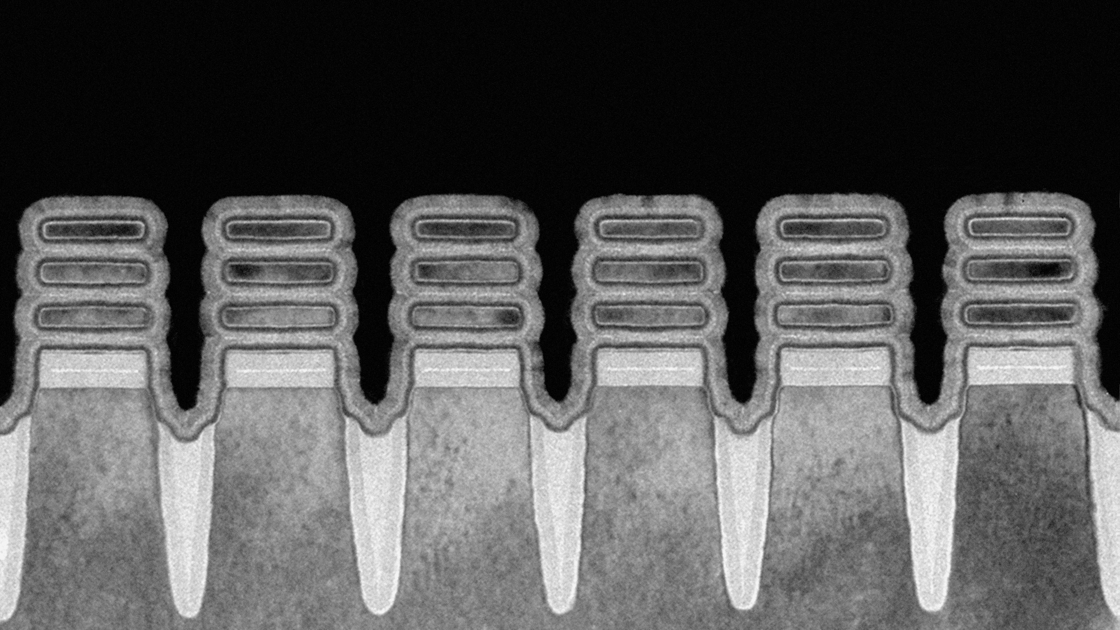
- Historic Density Milestone: IBM Research successfully prototyped the world’s first 2-nanometer (nm) gate-all-around (GAA) nanosheet test chip, packing a staggering 50 billion transistors onto a fingernail-sized footprint.
- Unprecedented Efficiency Gains: The architecture delivers up to 45 percent higher performance or 75 percent lower energy consumption compared to mainstream 7nm node chips currently dominating enterprise data centers.
- Capital Expenditure & Supply Chain Realignment: This breakthrough arrives amid intense capital allocation toward domestic semiconductor manufacturing, altering valuation multiples for legacy foundries and accelerating enterprise infrastructure scalability roadmaps.
- Strategic Sovereignty: Developed at IBM’s Albany NanoTech Complex, the milestone reinforces the critical race for technological self-sufficiency among Western economies and major tech conglomerates.
NEW YORK — In an epoch-defining leap for microelectronics, IBM Research fundamentally altered the trajectory of the global semiconductor industry by debuting the world’s first 2-nanometer (nm) test chip. Unveiled at the Albany NanoTech Complex on May 6, 2021, this technological tour de force crams an astonishing 50 billion transistors onto a die roughly the size of a fingernail. For enterprise technology leaders, chief financial officers, and sovereign policymakers navigating a complex web of supply chain vulnerabilities and escalating cloud compute workloads, IBM’s announcement represents far more than an academic triumph. It signals a tectonic shift in enterprise ROI, power-density management, and the macroeconomic valuation of silicon infrastructure.
The Physics of the Microscopic: Anatomy of a 2nm Breakthrough
Test Our Free AI & Tech Utilities Suite
Calculate LLM API token costs, analyze article dwell-time, or simulate tech DCA returns.
For decades, Moore’s Law—the empirical observation that the number of transistors on a microchip doubles roughly every two years—has faced mounting thermodynamic and quantum mechanical roadblocks. As lithography dimensions shrank below the 10nm threshold, traditional FinFET (Fin Field-Effect Transistor) architectures began to suffer from severe current leakage and diminishing returns in operational efficiency. Enter IBM Research and its pioneering implementation of a gate-all-around (GAA) nanosheet transistor architecture.
By vertically stacking distinct silicon nanosheets, IBM’s engineering team circumvented the physical limitations of planar and fin-based designs. This innovative configuration allows electrical current to pass more freely through the channel while exerting absolute electrostatic control over the gate. The result of this microscopic engineering is a die boasting 50 billion microscopic switches, each scaled to dimensions that push the very boundaries of atomic manipulation.
To contextualize the scale: at 2nm, individual channels are only a few nanometers thick—equivalent to a fraction of a DNA strand. This hyper-scaling enables chip designers to pack vastly superior compute capabilities into mobile devices, hyperscale cloud data centers, edge computing nodes, and autonomous systems without generating catastrophic thermal output. According to empirical benchmarks released by IBM, a 2nm processor can achieve either a 45 percent performance boost at identical power draw, or a 75 percent reduction in power consumption compared to standard 7nm node chips deployed across contemporary enterprise servers.
Macroeconomic Impact: Capital Allocation, Valuation Multiples, and Foundry Economics
Beyond the cleanrooms of upstate New York, IBM’s 2nm milestone carries profound implications for global financial markets and corporate capital allocation. Semiconductor manufacturing is arguably the most capital-intensive sector in the global economy, characterized by soaring capital expenditures (CapEx), stringent regulatory compliance mandates, and high market liquidity requirements.
In an era where digital transformation dictates enterprise valuation multiples, power efficiency is directly tied to the bottom line. Hyperscale cloud providers—such as Amazon Web Services, Microsoft Azure, and Google Cloud—spend billions of dollars annually on electricity to cool sprawling server farms. A 75 percent reduction in energy consumption at the silicon level translates directly into depressed operating expenditures, expanded EBITDA margins, and accelerated infrastructure scalability.
| Metric / Specification | Mainstream 7nm Node Chips | IBM Research 2nm Test Chip |
|---|---|---|
| Transistor Density | Standard enterprise density (~100M-150M transistors/mm²) | 50 Billion transistors on a fingernail-sized die |
| Transistor Architecture | FinFET (Fin Field-Effect Transistor) | Gate-All-Around (GAA) Nanosheet Architecture |
| Performance vs. 7nm | Baseline (1x) | Up to 45% increase at the same power |
| Energy Efficiency vs. 7nm | Baseline (1x) | Up to 75% lower energy consumption |
| Primary Target Applications | Consumer mobile, standard data center workloads | AI workloads, hyperscale cloud, 6G, autonomous systems |
Furthermore, the geopolitical dimension of semiconductor manufacturing cannot be overstated. With supply chain bottlenecks and geopolitical tensions threatening international trade routes, Western economies have aggressively pursued technological self-reliance. IBM’s successful prototyping at its Albany facility—supported by a robust public-private research ecosystem—demonstrates that advanced R&D remains a critical defensive moat for Western technology leadership. As venture capital and private equity firms recalibrate their portfolios, semiconductor innovation and advanced packaging technologies are commanding premium risk-adjusted valuations.
Industry Repercussions: Who Wins, Who Loses
Every major technological paradigm shift creates clear winners and losers across the industrial ecosystem. The debut of the 2nm test chip reshapes the competitive dynamics for legacy foundries, fabless designers, and enterprise end-users.
- The Winners: Advanced foundry pioneers capable of licensing or adapting GAA architectures stand to capture immense market share. Fabless artificial intelligence and machine learning hardware startups will leverage extreme density nodes to train massive large language models with a fraction of the carbon footprint and energy overhead.
- The Transitioning Incumbents: Traditional chipmakers tied to older lithography nodes face compressed margins and immense pressure to upgrade their fabrication plants (fabs). The transition from FinFET to GAA requires multi-billion-dollar retooling of extreme ultraviolet (EUV) lithography equipment, testing the balance sheets of secondary players.
- Enterprise End-Users: Chief Information Officers (CIOs) stand to benefit from denser, cooler, and faster hardware. Whether running complex financial risk-modeling algorithms, real-time fraud detection engines, or generative AI models, enterprise software will run on hardware that eliminates historical thermal bottlenecks.
Frequently Asked Questions (People Also Ask)
What is a Gate-All-Around (GAA) nanosheet architecture, and why is it superior to FinFET?
Gate-All-Around (GAA) architecture is a design methodology where the gate material completely surrounds the channel on all four sides, offering vastly superior electrostatic control compared to older FinFET designs where the gate surrounds the channel on only three sides. This eliminates detrimental current leakage, enabling significantly higher transistor density and optimized power-performance trade-offs at sub-3nm nodes.
How does IBM’s 2nm chip impact everyday consumer devices and enterprise servers?
For consumers, a 2nm mobile processor could theoretically quadruple battery life or deliver blazing-fast processing speeds while keeping smartphones remarkably cool. For enterprise data centers, the technology translates into dramatically lower power consumption, allowing data center operators to pack vastly more compute power into existing server racks without exceeding thermal and electrical limits.
When will 2nm chips be commercially available in the market?
While IBM successfully demonstrated functional prototyping of the 2nm test chip in May 2021, commercial manufacturing and volume production by semiconductor foundries typically require an 18-to-36-month timeline to transition from laboratory wafers to high-yield mass production. Foundries utilize these test chips to refine lithography masks, optimize chemical-mechanical planarization, and secure fab readiness.
Is IBM manufacturing these chips independently for the open market?
IBM operates on a research-and-development model rather than functioning as a high-volume commercial foundry like TSMC or Samsung. IBM typically licenses its breakthrough semiconductor designs and intellectual property to manufacturing partners, integrating these innovations into its own high-end enterprise server systems, such as the IBM zSystems mainframe line.
Future Outlook: The Road Beyond 2nm
As the microelectronics industry digests the implications of IBM’s 50-billion-transistor milestone, the horizon is already shifting toward even more exotic materials and structural paradigms. Research labs are actively exploring sub-1nm nodes, complementary metal-oxide-semiconductor (CMOS) scaling extensions, carbon nanotube transistors, and three-dimensional monolithic integration.
For institutional investors and enterprise technology strategists, the key performance indicators to monitor over the next 24 to 36 months will include EUV lithography yield rates, foundry capital expenditure announcements, and the commercial rollout of GAA-based silicon by major foundry partners. IBM’s 2nm breakthrough has definitively proven that Moore’s Law is not dead—it has simply evolved, demanding deeper capital investment, more sophisticated materials science, and uncompromising engineering brilliance to chart the silicon endgame.