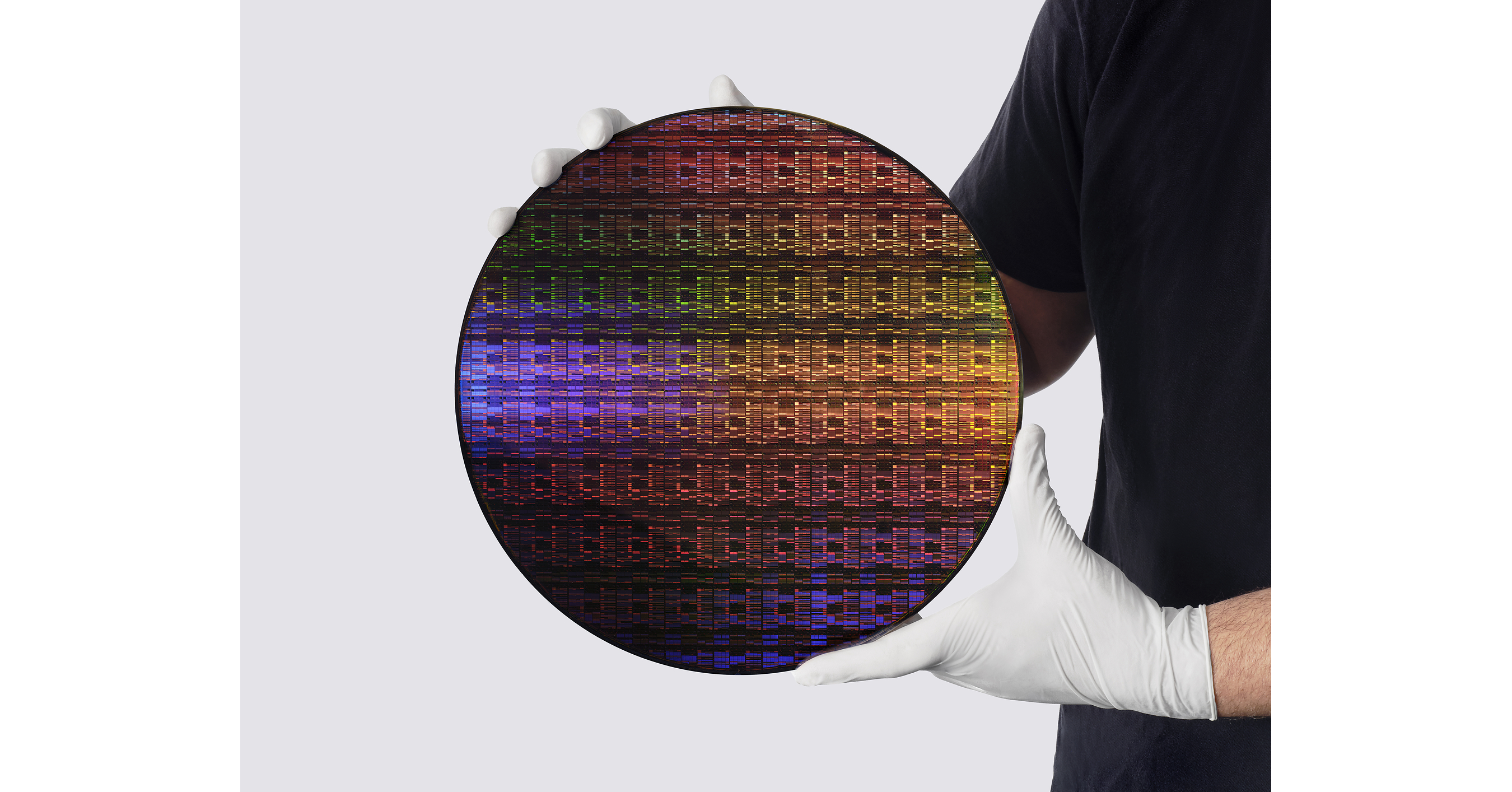
NEW YORK & BENGALURU — In a move that redrafts the geopolitical and technological roadmap of the global semiconductor industry, IBM Research has officially debuted the world’s first sub-1 nanometer (nm) silicon chip technology. Built on a radical, proprietary 3D architecture dubbed "Nanostack," the breakthrough effectively bypasses the looming physical limitations of classic silicon scaling, promising to unleash unprecedented computational power while throwing a lifeline to an artificial intelligence sector facing an acute energy crisis.
According to IBM’s technical brief released on June 25, 2026, this new architecture manages to pack an astonishing 100 billion transistors onto a slice of silicon no larger than a human fingernail. For comparison, the industry’s current state-of-the-art commercial processors, built on 3-nanometer processes, house roughly half that density. The announcement marks the most significant leap in semiconductor physics since the introduction of Gate-All-Around (GAA) nanosheets, positioning Big Blue as the undisputed vanguard of deep-tech R&D.
The Physics of the Breakthrough: What is 'Nanostack'?
For the past decade, material scientists have warned that semiconductor scaling was grinding to a halt. As gate lengths shrink toward 1 nanometer, quantum tunneling—a phenomenon where electrons uncontrollably leak through microscopic silicon barriers—threatened to render chips unstable, inefficient, and excessively hot.
IBM’s "Nanostack" architecture solves this fundamental bottleneck by transitioning from horizontal scaling to a highly sophisticated vertical 3D integration. Instead of placing nanosheets side-by-side, Nanostack layers multiple active transistor channels vertically with atomically precise insulating barriers. This allows IBM to reduce the physical footprint of the cell while maintaining robust electrostatic control over the channel, virtually eliminating current leakage.
Key Architectural Innovations:
- Vertical Channel Integration: Stacking up to six gate-all-around nanosheets vertically within a single transistor structure, doubling the active surface area without expanding the horizontal footprint.
- Atomically Precise Insulating Layers: Implementing novel 2D materials as ultra-thin insulators to prevent quantum tunneling between stacked channels.
- Backside Power Delivery Network (BPDN): Separating the power delivery circuitry from the data-transmitting signal lines by moving power distribution to the underside of the wafer, reducing voltage droop by up to 30%.
- Low-Temperature Molecular Bonding: Utilizing a proprietary low-heat process to stack and fuse silicon layers without damaging pre-fabricated underlying circuits.
Comparing the Generations: The Quantum Leap in Metrics

To fully appreciate the magnitude of IBM’s sub-1nm breakthrough, it must be measured against the current commercial standard (3nm) and the next-generation nodes currently under development by foundry giants like TSMC, Samsung, and Intel.
| Metric / Node | 3nm Class (Current Std.) | 2nm Class (Upcoming) | IBM Sub-1nm Nanostack |
|---|---|---|---|
| Transistor Density (Per mm²) | ~150–220 Million | ~280–310 Million | ~650+ Million |
| Total Transistors (Fingernail Size) | ~30–50 Billion | ~65–75 Billion | ~100 Billion |
| Power Reduction (At Constant Speed) | Baseline | ~25–30% Reduction | ~75% Reduction |
| Performance Gain (At Constant Power) | Baseline | ~15–20% Increase | ~45% Increase |
Resolving the AI Power Crisis
The timing of IBM’s disclosure could not be more critical. The generative AI boom has triggered an insatiable demand for computing power, pushing utility grids to their absolute limits. Data centers hosting large language models (LLMs) are projected to consume more than 1,000 terawatt-hours of electricity globally by the end of the decade—roughly equivalent to the entire energy consumption of Japan.
By offering a 75% reduction in power consumption compared to existing 3nm chips at identical operational speeds, IBM’s sub-1nm technology targets this systemic bottleneck. If deployed at scale across global cloud hyperscalers, this architecture could theoretically slash data center carbon footprints by millions of metric tons annually while enabling complex models to run locally on consumer edge devices, such as smartphones and autonomous vehicles, without draining their batteries.
"This isn't just about making computers faster; it is about keeping the AI revolution ecologically and economically viable," says Dr. Arati Prabhakar, a leading semiconductor analyst. "We were rapidly approaching a power wall where the cost of cooling data centers would outpace the financial returns of the software running inside them. Sub-1nm architecture delays that wall indefinitely."
The Road to Commercialization: Geopolitical Ripples
While IBM operates as a research powerhouse rather than a commercial volume foundry, its technological blueprints dictate the future roadmap of the entire industry. Historically, IBM partners with manufacturing behemoths to bring its research to the physical market—similar to how its 2nm breakthrough in 2021 paved the way for TSMC's and Intel's current production timelines.
Foundry executives in Hsinchu, Seoul, and Oregon are reportedly already analyzing the licensing potential of the Nanostack patent portfolio. However, integrating sub-1nm nodes into high-volume manufacturing will require massive capital expenditure. It will necessitate next-generation High-NA (High Numerical Aperture) Extreme Ultraviolet (EUV) lithography systems from Dutch monopoly ASML, which currently retail for upwards of $380 million per machine.
Market analysts expect that initial commercial implementation of IBM’s sub-1nm patents will not hit mass production until at least 2029 or 2030, given the extensive re-tooling required for global fabrication plants (fabs). Nevertheless, the announcement fires a massive warning shot across the bow of competitors, signaling that the race to dominate the post-silicon era has officially begun.
Frequently Asked Questions (FAQ)
1. When will sub-1nm chips be available in consumer devices?
While the technology has been successfully demonstrated in IBM's state-of-the-art Albany NanoTech Complex, mass commercialization is projected for 2029–2030. Foundries like TSMC, Intel, and Samsung must first integrate IBM's "Nanostack" patents into their upcoming high-volume fabrication facilities, which requires adopting ASML's High-NA EUV lithography tools.
2. How does "Nanostack" solve the problem of quantum tunneling?
Quantum tunneling occurs when chips become so small that electrons "leak" through physical barriers, causing chip failure. Nanostack solves this by stacking the transistor channels vertically and separating them with novel, atomically precise 2D insulating materials. This vertical configuration gives the transistor gates significantly tighter electrostatic control over the electron flow, preventing leaks even at sub-1nm dimensions.