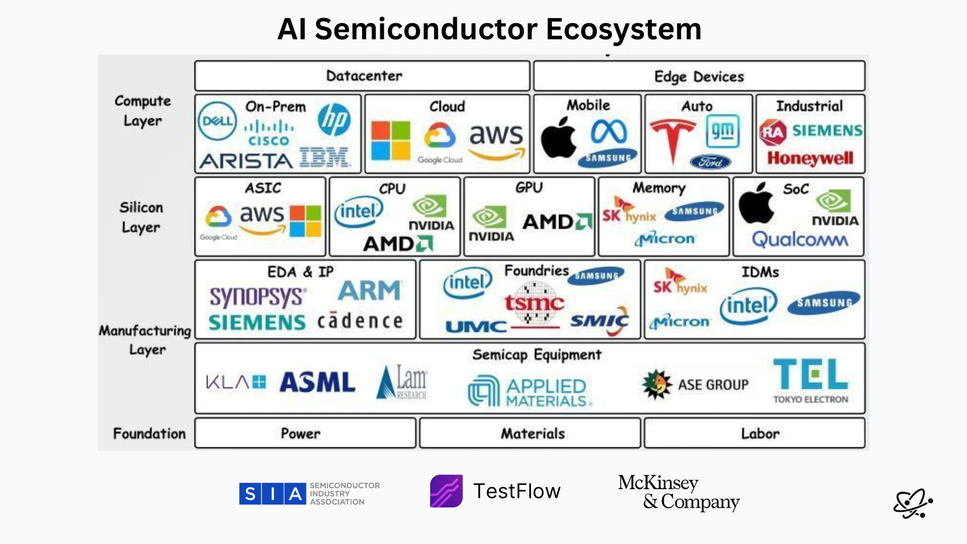
WASHINGTON, LONDON & TOKYO — June 15, 2026 — Bisinfotech Wire / Financial Technology Investigative Desk — The global semiconductor sector has officially crossed the threshold into a new economic and technological epoch. Accelerated by relentless enterprise demand for generative artificial intelligence, domain-specific silicon, and unprecedented compute density, the semiconductor market is converging on the $1 trillion annual valuation mark years ahead of mid-decade institutional projections.
What began as a tactical land grab for discrete graphics processing units (GPUs) has matured into an institutional overhaul of cloud compute architecture, lithographic physics, and global capital allocation. As leading-edge foundries push sub-2-nanometer process nodes into high-volume manufacturing (HVM), the industry faces a fundamental truth: incremental planar scaling is dead. The next decade of technology earnings, sovereign digital infrastructure, and enterprise productivity gains will be decided by radical breakthroughs in Gate-All-Around (GAA) transistor topologies, Backside Power Delivery Networks (BSPDN), High-Bandwidth Memory 4 (HBM4), and Co-Packaged Optics (CPO).
Executive Takeaways
- The $1 Trillion Frontier: Driven by hyperscaler infrastructure expansion and sovereign AI programs, total semiconductor industry revenues are pacing toward $1 trillion, reshaping capital expenditure priorities across major technology enterprises.
- Architectural Shift to Sub-2nm Nodes: Gate-All-Around (GAA) nanosheet transistors paired with Backside Power Delivery Networks (BSPDN) have moved from pilot production into high-volume manufacturing, overcoming legacy thermal and parasitic capacitance bottlenecks.
- The Memory & Interconnect Paradigm: HBM4 transitions the memory interface to a 2048-bit bus width utilizing advanced logic base dies, while Co-Packaged Optics (CPO) displaces copper at the rack scale to eliminate the data center "energy wall."
- Capital Allocations & Valuation Dynamics: Leading-edge wafer costs exceeding $28,000 at sub-2nm nodes are consolidating market power among a tightly integrated triopoly of foundries, while accelerating hyper-scaler migration toward custom domain-specific ASICs.
Part I: The Macroeconomic Supercycle & Hyperscaler Capital Allocation

The macroeconomic trajectory of the semiconductor industry in 2026 reflects a profound structural realignment. Global enterprise expenditures are no longer driven purely by consumer hardware cycles or traditional enterprise IT refresh cadences. Instead, capital expenditure (CapEx) budgets at hyperscale cloud providers—including Microsoft, Alphabet, Amazon, Meta, and ByteDance—have anchored the semiconductor value chain in an unprecedented multi-year investment cycle.
Capital deployment models indicate that hyperscaler CapEx allocation toward AI infrastructure and advanced compute silicon has exceeded $220 billion in 2026 alone. Institutional equity analysts and fixed-income credit desks are recalibrating valuation multiples based on a firm's ability to demonstrate tangible enterprise Return on Investment (ROI) from these infrastructure investments. As cloud service providers (CSPs) face tightening power grids and physical real estate limits, the strategic objective has shifted from raw chip procurement to energy-efficiency maximization per teraflop.
This economic reality has fractured the traditional commercial chip model. While merchant accelerator vendor platforms remain dominant for generalized model training, hyperscalers are aggressively expanding their custom Application-Specific Integrated Circuit (ASIC) portfolios. Custom silicon now accounts for over 28% of all deployed hardware in tier-1 cloud facilities, forcing fabless design firms and integrated device manufacturers (IDMs) to re-evaluate their competitive moats and long-term margin profiles.
Part II: Physics at the Edge: GAAFET, BSPDN, and High-NA EUV
At the physical scaling frontier, 2026 marks the absolute transition away from legacy FinFET (Fin Field-Effect Transistor) structures. As channel lengths shrank below 3nm, short-channel effects, threshold voltage variability, and quantum mechanical leakage currents severely compromised power-performance-area (PPA) metrics. The solution—now fully deployed across commercial foundries—is the Gate-All-Around Nanosheet FET (GAAFET).
GAAFET and Complementary FET (CFET) Roadmaps
GAA architecture wraps the conductive gate entirely around thin horizontal ribbons of silicon, restoring electrostatic control over the channel. This multi-bridge channel (MBCFET) approach enables chip designers to tune nanosheet widths, balancing dynamic capacitance against drive current. Foundries are already previewing the next logical evolutionary leap: Complementary FET (CFET), which stacks n-channel and p-channel transistors vertically on top of one another, effectively doubling logic density without reducing feature sizes further.
Backside Power Delivery Networks (BSPDN)
Concurrently, the industry has resolved one of physical design's most persistent bottlenecks: signal and power line congestion on the wafer's front side. Historically, both signaling lines and power delivery rails competed for space in the upper metal interconnect stacks (BEOL), leading to significant IR drop (voltage drop) and parasitic resistance. Through Backside Power Delivery Networks—known commercially under terms such as TSMC’s Super Power Rail and Intel’s PowerVia—power delivery is redirected entirely to the reverse side of the silicon wafer using buried power rails (BPR) and extreme-aspect-ratio Through-Silicon Vias (TSVs).
This decoupling yields dramatic physical advantages:
- Standard cell height reduction of 15% to 20%, resulting in immediate die-size compression.
- Up to 12% operational speed gains due to diminished resistive voltage drops and cleaner power distribution.
- Substantial mitigation of cross-talk and capacitance between sensitive signal lines and high-current power traces.
High-NA EUV Commercial Deployment
Making these physical structures economically viable requires ASML's High-Numerical Aperture Extreme Ultraviolet (High-NA EUV) lithography systems. Featuring an anamorphic lens design with an aperture of 0.55 NA (up from 0.33 NA in standard EUV), these multi-hundred-million-dollar scanners allow single-exposure printing of features down to 8nm. By eliminating complex multi-patterning steps, High-NA EUV dramatically restores wafer yield stability, albeit at elevated capital expenditures that only the top tier of foundries can finance.
Part III: Solving the "Memory Wall" and Interconnect Bottlenecks
Compute performance gains at the core level are rendered useless if memory bandwidth and chip-to-chip latency cannot scale in tandem—a phenomenon long known as the memory wall. In 2026, memory and packaging innovations have transitioned from supporting roles to the primary competitive differentiator in advanced compute systems.
The HBM4 Epoch and Logic Base Dies
High-Bandwidth Memory 4 (HBM4) represents a radical architectural break from its predecessors (HBM3 and HBM3e). To break through the bandwidth limitations of traditional 1024-bit physical interfaces, the HBM4 specification expands the interface to a 2048-bit wide bus. This wider bus requires an essential structural modification: the bottom "base" or "buffer" die of the memory stack is no longer fabricated on standard, low-cost DRAM processes. Instead, memory vendors have partnered directly with leading-edge logic foundries to manufacture the HBM4 base die on advanced 3nm and 4nm logic nodes.
By using sub-5nm logic processes for the memory base die, designers can integrate custom on-die test structures, low-power physical layers (PHY), and even near-memory compute capabilities. This allows direct micro-bump-less bonding (such as copper-to-copper hybrid bonding) directly onto the host SoC or GPU, delivering memory bandwidths exceeding 2.0 Terabytes per second per stack while reducing active interface power consumption by over 30%.
Advanced Packaging, Chiplets, and Co-Packaged Optics (CPO)
The industry's shift away from monolithic dies to disaggregated "chiplet" architectures is now absolute. Through 2.5D and 3D heterogeneous integration—utilizing silicon interposers, organic substrates, and direct die-to-die stacking—manufacturers are assembling complex compute platforms containing hundreds of billions of transistors across isolated die tiles.
However, as cluster sizes scale to thousands of interconnected processing units inside data centers, metallic copper interconnects have hit physical dissipation limits. Electric current flowing through high-speed copper traces generates prohibitive thermal dissipation and signal attenuation at frequencies above 112 Gbps per lane. The industry's answer is Co-Packaged Optics (CPO). By mounting silicon photonics engines directly onto the same multi-chip package substrate as the compute die, electrical signals are converted to optical signals directly at the package edge. This transition slashes interconnect power overhead by up to 70% and enables rack-scale compute fabrics to operate with near-zero latency penalty across massive optical switches.
Data Breakdown: 2026 Semiconductor Metric Matrix
The comparative table below illustrates the structural performance, architectural, and financial shifts across leading-edge node generations and memory interfaces as of mid-2026.
| Technology Vector | Legacy Standard (3nm Class / HBM3e) | 2026 Commercial Baseline (Sub-2nm Class / HBM4) | Primary Structural Driver | Enterprise & Financial Impact |
|---|---|---|---|---|
| Transistor Architecture | FinFET / Early Nanosheet GAA | Advanced GAAFET / Vertical CFET Stack | Channel electrostatic control recovery | +15% clock frequency at equivalent power envelopes |
| Power Routing Topology | Front-Side BEOL Metallization Stack | Backside Power Delivery Network (BSPDN) | Buried Power Rails & Reverse-side TSVs | 15–20% standard cell density compression; reduced IR drop |
| Lithography Exposure | Standard EUV (0.33 NA, Multi-patterning) | High-NA EUV (0.55 NA Anamorphic) | Single-exposure sub-10nm feature resolution | Reduces mask count; raises fab entry CapEx threshold |
| Memory Architecture | HBM3e (1024-bit bus, DRAM Base Die) | HBM4 (2048-bit bus, Advanced Logic Base Die) | Foundry-fabricated sub-5nm buffer die | >2.0 TB/s per stack bandwidth; 30% energy efficiency gain |
| Package Interconnect | High-Density Copper Traces (112G SerDes) | Co-Packaged Optics (CPO Silicon Photonics) | Direct die-edge electro-optical conversion | 70% reduction in rack-to-rack interconnect power draw |
| Economics & Pricing | ~$18,000–$20,000 per wafer | >$28,000 per wafer (sub-2nm) | High-NA EUV capital depreciation & yield costs | Accelerates migration to custom domain-specific ASICs |
Industry & Market Implications: Winners, Losers, and Geopolitical Realities
The shifts unfolding in 2026 carry profound implications for public market equity valuations, venture capital allocation, and geopolitical risk strategy.
The Foundry Triopoly and Capital Intensity Moats
The capital expenditure required to remain competitive at the leading edge has created an almost insurmountable barrier to entry. Developing a fully operational sub-2nm gigafab today requires upwards of $20 billion in capital outlay, heavily weighted toward ASML High-NA EUV toolsets, cleanroom automation, and multi-layer Metrology equipment. This dynamics narrows the leading-edge foundry market down to three global entities: TSMC, Samsung Foundry, and Intel Foundry Services (IFS). Tier-2 foundries have effectively abandoned leading-edge logic scaling, pivoting instead to high-margin mature nodes, legacy analog, and power electronics (GaN/SiC) for automotive and industrial platforms.
Geopolitical Redundancy Meets Operational Cost Realities
The policy push for geographic supply chain diversification—driven by the U.S. CHIPS Act, European Chips Act, and Japanese sovereign subsidies—has achieved physical reality in 2026. Advanced fabrication facilities in Arizona, Ohio, Dresden, and Kumamoto are ramping initial production runs. However, initial yield ramps at these international nodes have highlighted structural margin headwinds. Operating expenses in Western jurisdictions—driven by skilled labor deficits, elevated utility costs, and complex regulatory compliance frameworks—have resulted in a 15% to 25% cost premium over historical Taiwanese and South Korean foundry operations. Enterprise customers are consequently navigating bifurcated pricing models: paying a premium for geographically secure, redundant silicon versus standard Asian foundry runs.
Power Electronics Scaling: SiC and GaN Beyond Compute
While logic processors capture media coverage, power management silicon is undergoing an equally critical evolution. Wide-bandgap semiconductors—specifically Silicon Carbide (SiC) and Gallium Nitride (GaN)—are displacing traditional silicon IGBTs across data center Power Distribution Units (PDUs), electric vehicle architectures, and renewable grid infrastructures. As hyperscale data center power requirements balloon into multi-gigawatt territories, the deployment of 800V and 1200V SiC/GaN power conversion systems has become essential to prevent grid-level distribution losses.
Frequently Asked Questions (People Also Ask)
What is driving the semiconductor market toward the $1 trillion valuation mark in 2026?
The trajectory toward $1 trillion is fueled by the rapid deployment of artificial intelligence infrastructure across global cloud enterprise networks, sovereign digital initiatives, and the ubiquity of high-density compute across automotive, industrial, and consumer sectors. Higher average selling prices (ASPs) for advanced sub-2nm nodes, premium HBM4 stacks, and high-density heterogeneous packaging have structural expanded total sector revenue potential.
How does Backside Power Delivery Network (BSPDN) differ from traditional front-side power routing?
Traditional semiconductor architectures deliver electric power through the same front-side metal layers (BEOL) that carry data signals, causing routing congestion, signal interference, and voltage drops. BSPDN moves all power distribution lines to the physical backside of the silicon wafer using buried power rails and through-silicon vias. This decouples signal lines from power paths, increases transistor logic density by up to 20%, and improves overall chip clock speeds and power efficiency.
Why is HBM4 considered a structural shift compared to prior memory generations like HBM3e?
HBM4 doubles the physical interface width from 1024 bits to 2048 bits and fundamentally alters how the base "buffer" die is made. Instead of using standard DRAM processes, HBM4 base dies are manufactured on advanced 3nm or 4nm logic foundry processes. This allows memory makers to integrate advanced logic features, micro-bump-less hybrid bonding, and custom energy-efficient physical layer interfaces directly into the memory stack, overcoming long-standing data bandwidth bottlenecks in AI compute cluster designs.
How are custom hyperscaler ASICs altering the competitive landscape for merchant GPU suppliers?
Hyperscale cloud providers are designing custom domain-specific processors (ASICs) optimized specifically for their internal workload profiles, recommendation engines, and targeted AI inference tasks. By bypassing the profit margins and software overhead of merchant accelerators, hyperscalers can achieve superior power efficiency and lower total cost of ownership (TCO). While merchant GPUs continue to lead in general-purpose model training, custom ASICs are rapidly taking market share in scale-out inference and specialized cloud compute applications.
Future Outlook: Strategic Milestones to Watch (2026–2030)
As the semiconductor industry cements its position as the foundational currency of the global digital economy, the strategic roadmap through 2030 will be defined by execution across several critical technological milestones:
- Commercialization of Complementary FET (CFET): Anticipated for risk production by late 2027, CFET will replace horizontal nanosheets with vertically stacked n-FET and p-FET devices, unlocking a new wave of logic density without requiring proportional feature shrinkage.
- Full Optical Compute Planes: As silicon photonics matures from chip-to-chip interfaces to die-to-die and intra-die optical interconnects, fully optical switch fabrics will become standard in top-tier exascale processing environments.
- Monolithic 3D Integration: Moving beyond micro-bump interconnects, direct hybrid bonding at sub-micron pitches will enable true 3D memory-on-logic stacking, diminishing the latency wall between high-speed cache and logic blocks.
- Power Supply Bottlenecks: Fabs and data centers alike will face increasing scrutiny over local electrical grid capacities. The integration of advanced power management systems, high-voltage GaN/SiC power converters, and on-chip power regulation will be mandatory for future infrastructure deployments.
The semiconductor industry of 2026 is no longer just a sector within the technology asset class—it is the strategic bedrock of enterprise capital strategy, industrial policy, and global sovereign security. Institutions that effectively manage the capital allocation demands, physics challenges, and geopolitical risks inherent to this sub-2nm era will capture the dominant share of economic value across the next decade of digital transformation.