NEW DELHI & BENGALURU — On May 5, 2026, the Union Cabinet sanctioned two additional high-stakes semiconductor fabrication and assembly installations, marking an aggressive acceleration of New Delhi’s multi-billion-dollar effort to re-engineer global microelectronics manufacturing. Coming nearly five years after the initial launch of the ₹76,000-crore ($9.1 billion) India Semiconductor Mission (ISM), the latest approvals underscore a decisive tactical shift: transitioning the subcontinent from an intellectual cradle for fabless design talent into a battle-tested hardware power capable of absorbing Western supply-chain de-risking.
The global semiconductor industry, historically consolidated within the crosshairs of geopolitical flashpoints in the Taiwan Strait and East Asia, is facing structural decentralization. India’s aggressive intervention—leveraging a 50% central fiscal capital expenditure (capex) subsidy matched by up to 20% to 25% in state-level top-ups—has systematically altered corporate hurdle rates. Multinationals and domestic conglomerates are no longer evaluating India as an exploratory outpost; it has evolved into a strategic hedge backed by state-sponsored balance sheets.
Executive Takeaways
- Regulatory Acceleration: The Union Cabinet’s May 5, 2026 approvals expand India’s verified project pipeline beyond basic Outsourced Semiconductor Assembly and Test (OSAT) facilities into commercial-scale 28nm-to-40nm complementary metal-oxide-semiconductor (CMOS) logic and wide-bandgap compound semiconductors (SiC/GaN).
- Sovereign Capital Subsidization: The central government's 50% pari-passu fiscal support dramatically compresses depreciation-heavy payback periods, lifting projected project internal rates of return (IRR) from sub-12% thresholds to enterprise-grade viability above 19%.
- Infrastructure and Yield Realities: The sector now confronts execution bottlenecks. Facility uptime hinges on dedicated ultra-pure water (UPW) plants, redundant gigawatt-scale green grid interconnections, and hazardous specialty-gas supply corridors across Gujarat, Assam, and Tamil Nadu.
- Strategic Bifurcation: New Delhi has pragmatically abandoned the immediate race for sub-3nm extreme ultraviolet (EUV) leading-edge nodes, positioning domestic manufacturing to corner the industrial, automotive, and telecommunications volume markets where global fab utilization rates remain consistently above 85%.
The Anatomy of the Push: From Fabless Design to Front-End Silicon
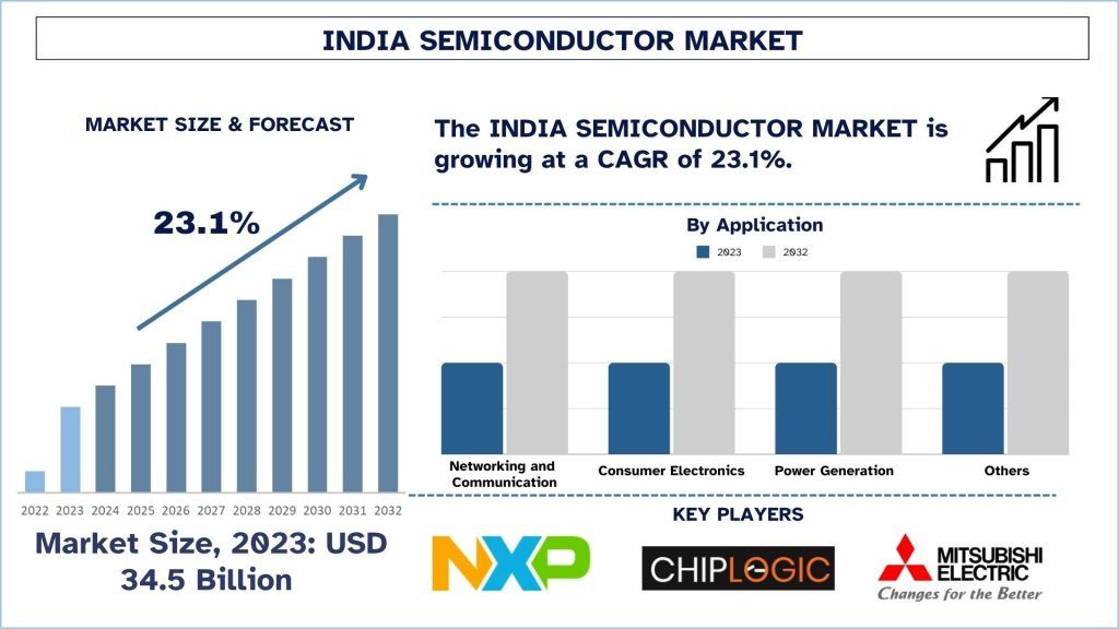
For more than three decades, India has functioned as the foundational back-office of the global semiconductor intellectual property (IP) complex. More than 20% of the world’s chip design engineers—spanning teams at Qualcomm, Intel, NVIDIA, and Texas Instruments—operate from campuses in Bengaluru, Hyderabad, and Noida. However, capturing structural value requires physical wafer fabrication, where gross margins routinely touch 50% and national sovereignty over secure silicon is guaranteed.
The May 5 Cabinet approvals deliver capital commitments directly into the industrial-grade manufacturing tier. Anchored by domestic champions partnering with seasoned global technology providers, the approved projects bridge the missing link between local design architectures and physical delivery. The expansion program strategically targets trailing and mature nodes (28nm to 65nm), which command over 45% of total addressable market (TAM) volume worldwide and drive electrification across the automotive, power management, industrial IoT, and consumer electronics segments.
By underwriting the project finance stack with upfront capital grants rather than deferred tax credits, the Ministry of Electronics and Information Technology (MeitY) has decoupled fab construction from traditional sovereign market credit risks. This dynamic has drawn heavy industrial conglomerates—groups capable of underwriting the prolonged capital expenditure cycles characteristic of semiconductor foundries—into strategic manufacturing consortia.
Fiscal Architecture: Enterprise ROI and CapEx Absorption
Constructing a greenfield semiconductor fab requires unprecedented capital intensity. A modern fab facility burns through $3 billion to $10 billion in capital expenditure, of which up to 70% is earmarked for advanced cleanroom equipment and deep ultraviolet (DUV) lithography steppers sourced from monopolistic equipment vendors like ASML, Applied Materials, Lam Research, and Tokyo Electron. Without structural state mitigation, early-stage yield losses, depreciation curves, and high debt-service costs create prohibitive barriers to entry.
The financial architecture engineered under the India Semiconductor Mission counters this dynamic by deploying non-dilutive, direct capital subsidies:
- Front-End Sovereign Parity: The Union Government covers 50% of the project’s eligible capital expenditure directly on a pari-passu reimbursement model, distributing cash outlays in lockstep with construction and equipment-procurement milestones.
- Sub-National Arbitrage: Competitive federalism has driven industrial states—principally Gujarat, Maharashtra, Karnataka, and Tamil Nadu—to compete via supplementary incentive matrices. These include an additional 20% to 25% capex subsidy, subsidized land acquisition, 20-year stamp duty exemptions, and discounted industrial tariffs for electrical power and industrial water supply.
- Depreciation Compression: By insulating investors from up to 70%–75% of baseline physical asset capex, the statutory amortization timeline drops significantly. This structural insulation reduces the debt-servicing load, insulating the fab operator from global macroeconomic cyclical downturns and silicon pricing crashes.
Project Portfolio: India's Operational and Approved Semiconductor Landscape
The progression of the national semiconductor pipeline showcases a deliberate, tiered industrial roadmap: initial OSAT/ATMP volume deployment, followed by specialty foundries, progressing toward high-volume 300mm wafer fabrication.
| Entity / Joint Venture | Facility Type / Node Spec | Primary Location | Projected Outlay (USD) | Current Status (as of May 2026) |
|---|---|---|---|---|
| Tata Electronics / PSMC | Commercial Logic Fab (28nm, 40nm, 91nm) | Dholera, Gujarat | $10.9 Billion | Phase-1 Civil Construction; Tool-in Targeted H2 2026 |
| Micron Technology | ATMP / OSAT (DRAM & NAND Packaging) | Sanand, Gujarat | $2.75 Billion | Operational Phase-1; Commercial Shipments Commenced |
| CG Power / Renesas / Stars Micro | OSAT (Legacy & Advanced Packages) | Sanand, Gujarat | $915 Million | Cleanroom Fit-Out; Test Runs Slated Q4 2026 |
| Tata Semiconductor Assembly (TSAT) | Advanced Packaging (Flip-Chip, Fan-Out) | Jagiroad, Assam | $3.25 Billion | Foundations Complete; Cleanroom Infrastructure Underway |
| Kaynes Semicon | Industrial / Power Module OSAT | Sanand, Gujarat | $395 Million | Equipment Installation; Early-Stage Pilot Yields |
| Approved Consortia (Cabinet: May 5, 2026) | Specialty Compound Fab (SiC/GaN) & Analog | Tier-1 Industrial Corridor | Undisclosed / Multi-Billion | Site Allocation & Environmental Clearance Execution |
Supply-Chain Bottlenecks: Infrastructure Scalability and Operational Execution
While sovereign capital allocation mitigates balance-sheet vulnerabilities, the operationalization of semiconductor facilities presents unforgiving engineering hurdles. A commercial-scale 300mm wafer fab consumes between 3 to 5 million gallons of Ultra-Pure Water (UPW) daily, alongside continuous electrical baseloads exceeding 100 megawatts—where a power voltage sag lasting fractions of a second can ruin an entire production cycle worth millions of dollars.
India’s primary industrial corridors have historically grappled with infrastructural volatility. To counter this, state entities have isolated these fabrication clusters within specialized Special Economic Zones (SEZs):
- Dual-Grid Interconnections: Sites like Dholera and Sanand feature dedicated, micro-grid transmission infrastructure directly wired into high-capacity renewable installations, supported by synchronous condensers to eliminate frequency deviations.
- Specialty Chemical Supply Lines: Advanced wafer etching and cleaning demand electronic-grade chemicals (hydrofluoric acid, isopropyl alcohol, hydrogen peroxide) purified to parts-per-billion tolerances. India currently imports more than 90% of these specialty gases and reagents. Building domestic purification clusters adjacent to fabs is vital to avoid high-cost international cold-chain air freight.
- Yield Optimization Trajectories: In foundry economics, initial tool-in to commercial revenue run-rates typically suffers from protracted defect cycles. Indian fab operators must navigate steep learning curves to achieve industry-standard baseline yields above 88%–92%, a process dependent on experienced foundry management talent sourced largely from Taiwan, South Korea, and Europe.
Market Winners, Losers, and Strategic Realignment
The rapid expansion of India's state-subsidized semiconductor ecosystem alters industrial power dynamics across multiple sectors:
The Winners
- Domestic Industrial Conglomerates: Groups such as Tata and Murugappa are transforming into vertically integrated technological leaders, capturing margin across both raw component manufacturing and high-growth downstream consumption verticals (electric vehicles, renewable inverters, enterprise telecommunications).
- Global Semiconductor Equipment Vendors: ASML, Applied Materials, Lam Research, and KLA Corporation secure an expanding, government-subsidized demand vector for mature DUV systems, offsetting market softness in regions facing stricter export-control regimes.
- Automotive and Industrial Tier-1 Suppliers: Localized mature-node fabrication provides domestic automakers with inventory resilience, curtailing exposure to maritime transport disruptions and geopolitical trade restrictions.
The Challenged
- Regional Legacy Foundries: Unsubsidized second-tier mature-node foundries in Southeast Asia and parts of mainland China will encounter acute price competition as Indian fabs—heavily capitalized by state balance sheets—scale domestic volume production.
- State Balance Sheets: The persistent requirement for multi-billion-dollar state outlays places sustained pressure on public expenditure, making ongoing returns on invested capital (ROIC) an operational and political imperative.
Frequently Asked Questions (People Also Ask)
Why is India prioritizing mature nodes (28nm to 65nm) instead of cutting-edge sub-3nm technologies?
Mature nodes between 28nm and 65nm represent the operational core of industrial electronics, automotive computing, power infrastructure, and telecommunications gear. They account for the largest global volume share and do not require extreme ultraviolet (EUV) lithography systems, which are cost-prohibitive and subject to intense export licensing scrutiny. Developing mature nodes provides immediate domestic commercial uptake, mitigates operational complexity, and allows the domestic ecosystem to establish process stability before attempting capital-intensive leading-edge engineering.
How does India’s 50% fiscal subsidy compare to international incentive packages like the US CHIPS Act?
While the US CHIPS and Science Act ($52.7 billion) and the European Chips Act (€43 billion) utilize complex mixes of grants, loans, and loan guarantees often tied to variable regulatory conditions, India’s India Semiconductor Mission provides an uncompromising direct grant covering 50% of the project’s total eligible capital expenditure. When combined with state-level subsidies, total capital underwriting in India can offset 70% to 75% of initial project setup expenses, offering one of the highest cash-in-hand capital expenditure incentives in the world.
What are the primary logistical risks that could stall Indian fab execution?
The primary vulnerabilities center on the supply chain for electronic-grade chemicals, continuous water processing, and specialized engineering retention. Semiconductor fabs require access to ultra-pure reagents and bulk gases with purity levels exceeding 99.9999%, which India currently lacks the domestic capacity to refine at scale. Any delay in developing localized purification hubs requires reliance on long-distance logistics networks, elevating supply-chain failure risks and inventory holding costs.
How does India convert its existing fabless chip design workforce into foundry operations?
India hosts roughly 20% of the world’s chip design talent, but this expertise focuses on software-driven design architecture, logic simulation, and physical layout rather than metallurgy, wafer processing, and cleanroom physics. To close this operational gap, domestic operators are employing international foundry veterans, partnering via structured technology transfers with established players (e.g., PSMC), and instituting academic training pipelines across premier engineering institutes to build cleanroom manufacturing capabilities.
Future Outlook: Strategic Milestones for 2026–2030
The approval issued on May 5, 2026, marks the midpoint of India’s ten-year semiconductor transformation. Between late 2026 and mid-2028, the market will witness the initial tool-in and first commercial wafer runs from the Tata-PSMC Dholera fab, alongside initial revenue recognition across multiple greenfield OSAT and compound semiconductor facilities.
The strategic focus will inevitably shift toward the rollout of the "ISM 2.0" framework. This next legislative iteration is anticipated to expand funding mechanisms to incentivize the domestic chemical ecosystem, cleanroom consumable manufacturing, and proprietary intellectual property development. For global enterprise investors, sovereign capital managers, and tech leaders, India’s execution metrics over the next 24 months will clarify whether the subcontinent can successfully translate its design footprint into sustainable, high-yield commercial silicon fabrication.