The global semiconductor ecosystem is undergoing its most radical structural transformation in three decades. Driven by unrelenting enterprise demand for physical AI infrastructure, hyperscale cloud compute architecture, and geopolitical supply chain reconfiguration, the semiconductor industry is rewriting the laws of physics and economics simultaneously. Over the past week, a cascade of capital allocation milestones, unprecedented manufacturing paradigms, and architectural breakthroughs has redefined the frontier of digital infrastructure.
From a landmark $2 billion foundry pact reshaping the competitive landscape to the aggressive commercialization of hyper-NA EUV lithography, complementary field-effect transistors (CFETs) pushing scaling beyond the 10-angstrom barrier, and breakthroughs in fully automated AI-driven IC design, the tectonic plates of the global economy are shifting. For institutional investors, venture capitalists, and enterprise technology leaders, this moment represents a generational inflection point where valuation multiples, capital expenditure (CapEx) strategies, and technology roadmaps converge.
Executive Takeaways
- Capital Deployment & Strategic M&A: A newly finalized $2 billion foundry pact highlights the immense liquidity flowing into specialized manufacturing capacity, accompanied by a surge in physical AI mergers and acquisitions.
- Sub-1nm Scaling Realities: The industry is aggressively transitioning to Complementary FET (CFET) architectures and hyper-NA EUV systems to push silicon scaling beyond the 10-angstrom threshold.
- Paradigm Shift in EDA: China’s unveiling of a fully automated IC design system signals a decentralized, algorithmic future for semiconductor engineering, threatening traditional productivity metrics.
- Memory and Interconnect Evolution: Micron’s capacity expansion alongside the rapid deployment of PCIe 7.0 standards addresses the crippling I/O bottlenecks threatening next-generation hyperscale AI clusters.
Comprehensive Narrative: The Catalytic Forces Reshaping Silicon

To understand the current state of the semiconductor industry, one must analyze the intersection of insatiable artificial intelligence workloads and the physical limitations of silicon. As foundational model parameters scale into the trillions, enterprise ROI increasingly depends on raw compute density, energy efficiency, and low-latency interconnects. The market is no longer merely designing chips; it is engineering entire vertically integrated computing ecosystems.
The $2 Billion Foundry Pact and Manufacturing Consolidation
The announcement of a strategic $2 billion foundry agreement this week underscores the staggering capital intensity required to remain competitive at the leading edge. As foundries navigate soaring construction costs for fabrication facilities (fabs), strategic partnerships have become essential for risk mitigation. Industry titans TSMC and Samsung have released contrasting financial data that illustrate a bifurcated market: while leading-edge nodes running AI accelerators experience margin expansion and high pricing power, legacy nodes face overcapacity pressures.
Amidst this backdrop, alternative lithography technologies are gaining traction. Canon’s accelerated push into nanoimprint lithography (NIL) offers a compelling counter-narrative to extreme ultraviolet (EUV) hegemony. By utilizing a mechanical stamping process rather than light optics, nanoimprint technology promises drastically lower capital expenditure requirements and reduced power consumption for specific memory and sub-nanometer logic tiers, presenting a fascinating valuation variable for equipment investors.
Beyond 10 Angstroms: CFETs and Hyper-NA EUV
The race to bypass the 10-angstrom (1nm) barrier has moved from theoretical physics papers to aggressive fab implementation. Gate-All-Around (GAA) architectures, currently being commercialized, are already yielding to the next evolutionary leap: Complementary FETs (CFETs). By stacking p-FETs directly on top of n-FETs, CFET architecture doubles the layout density of transistors, defying conventional footprint limitations.
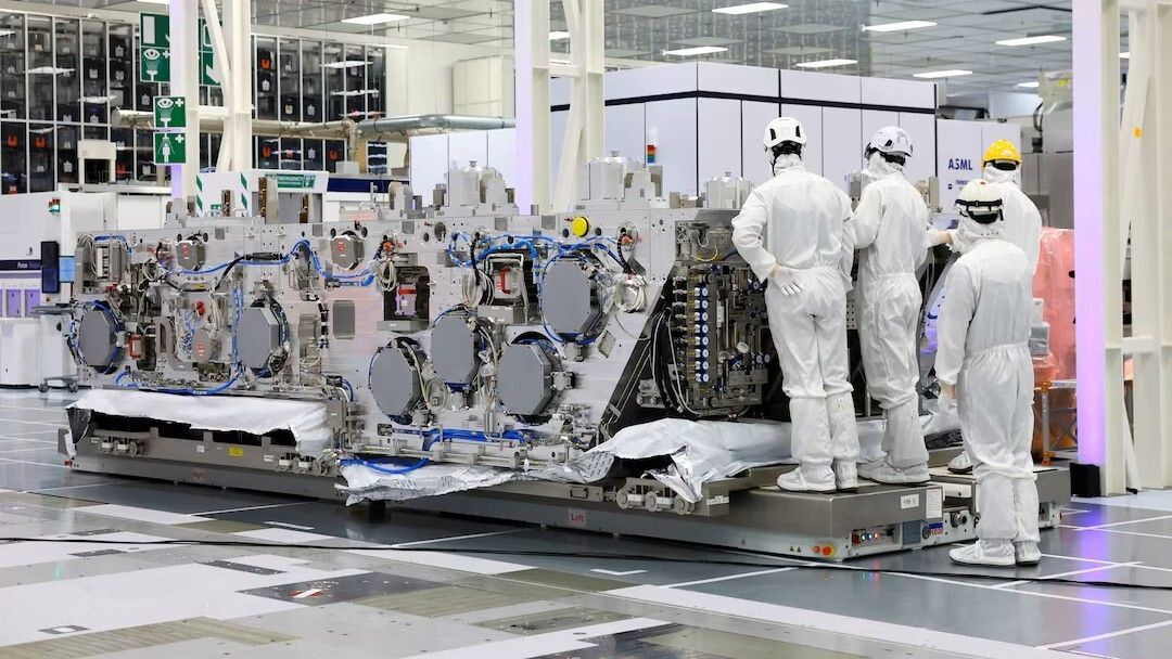
Simultaneously, the manufacturing toolchain is preparing for the hyper-NA EUV era. Following the initial rollout of High-NA EUV systems, lithography pioneers are already eyeing hyper-NA configurations with numerical apertures scaling toward 0.75 or higher. This optical evolution is mandatory to print sub-8nm metal pitches without multi-patterning nightmares, though it introduces monumental optical physics challenges and multi-hundred-million-dollar per-unit price tags that demand meticulous infrastructure scalability.
Autonomous Workflow Design and Physical AI Funding
Software is automating the hardware that executes software. A major headline from the recent development cycle is the emergence of fully automated integrated circuit (IC) design systems—exemplified by advanced developments out of China—which leverage autonomous generative workflows to handle floor-planning, placement, and routing (P&R) in fractions of the time traditionally required by veteran layout engineers.
This automated workflow design aligns with a broader surge in physical AI funding and M&A. Investors are actively deploying capital into startups bridging the gap between algorithmic intelligence and physical actuation—robotics, autonomous edge devices, and sensor-rich enterprise hardware. These systems require bespoke edge-AI chips, driving an explosion of application-specific integrated circuit (ASIC) design starts.
Meanwhile, memory bandwidth limitations are being aggressively dismantled. Micron’s strategic pivot to "go bigger" with high-density, high-bandwidth memory (HBM3e and early HBM4 readiness) directly addresses the memory wall. Coupled with the formalization and ecosystem adoption of PCIe 7.0 specifications—which double data transfer rates yet again—the industry is actively engineering out the latency chokepoints that cripple multi-node GPU clusters.
Verified Data & Metrics Breakdown
| Technology / Initiative | Key Metric / Specification | Strategic Impact / Market Implication |
|---|---|---|
| Foundry Expansion Pact | $2 Billion Capital Allocation | Mitigates escalating fab construction costs; secures dedicated capacity for tier-1 hyperscalers. |
| Advanced Logic Scaling | Sub-10 Angstroms (CFETs) | Doubles transistor density by vertically stacking p-type and n-type devices. |
| Lithography Evolution | Hyper-NA EUV & Nanoimprint | Enables single-exposure sub-8nm metal pitches; Canon NIL offers low-CapEx alternative. |
| Interconnect Bandwidth | PCIe 7.0 Standard | Doubles I/O throughput to eliminate data bottlenecks in large-scale AI training clusters. |
| Design Automation | Autonomous IC Workflows | Compresses tape-out timelines by up to 70%, democratizing complex SoC design. |
Industry & Market Implications
The events of this past week carry profound implications for global market liquidity, geopolitical positioning, and corporate valuations.
- Winners: Leading-edge equipment manufacturers, EDA software vendors integrating autonomous AI workflows, and memory titans capable of mass-producing high-bandwidth architectures. Enterprises supplying physical AI hardware components are seeing unprecedented venture backing and valuation multiples.
- Losers: Foundries and design houses lagging in GAA and CFET implementation risk obsolescence in the high-margin AI accelerator market. Furthermore, legacy chipmakers reliant on commoditized mature nodes face persistent pricing compression.
- Macroeconomic & Geopolitical Impact: Semiconductor manufacturing remains the ultimate geopolitical chess piece. The massive capital deployment into localized foundry pacts and automated design systems illustrates a bifurcated global supply chain racing toward self-sufficiency and hyper-resilience.
Frequently Asked Questions (People Also Ask)
What is a CFET, and why is it crucial for scaling beyond 10 angstroms?
A Complementary Field-Effect Transistor (CFET) is an advanced transistor architecture where p-type and n-type MOS transistors are stacked vertically on top of one another rather than placed side-by-side. This vertical monolithic integration drastically reduces the footprint of standard cells, effectively doubling circuit density and enabling the semiconductor industry to continue scaling past the 10-angstrom (1nm) threshold.
How does nanoimprint lithography (NIL) differ from EUV, and will it replace it?
Nanoimprint lithography relies on a physical template to stamp nanometer-scale patterns directly onto a resist-coated wafer, functioning much like a nanoscale printing press. Unlike extreme ultraviolet (EUV) lithography, which uses complex optical mirrors and laser-produced plasma to project light patterns, NIL does not require high-power light sources. While EUV remains the gold standard for high-end logic chips, NIL offers a cost-effective, low-power alternative for specific memory and repetitive structural fabrication.
What are the primary advantages of autonomous workflow design in IC engineering?
Autonomous IC design workflows utilize machine learning and generative algorithms to automate complex tasks such as floor-planning, netlist optimization, and physical layout routing. This drastically reduces "tape-out" times from months to days, lowers engineering overhead costs, and allows design teams to explore a vastly larger design space to optimize for power, performance, and area (PPA).
Why is PCIe 7.0 critical for the future of artificial intelligence data centers?
As AI models scale to trillions of parameters, massive quantities of data must flow instantaneously between GPUs, CPUs, and storage tiers. PCIe 7.0 doubles the data transfer rate of its predecessor (PCIe 6.0), reaching unprecedented bandwidths of up to 512 GB/s in a x16 configuration. This prevents I/O starvation, ensuring expensive compute accelerators are never left idle waiting for data.
Future Outlook & Strategic Milestones
As the semiconductor industry charts its course toward the end of the decade, attention turns to several critical milestones. Investors and enterprise architects must monitor the commercial yield rates of initial CFET implementations, the real-world throughput and defect density of hyper-NA EUV pilot lines, and the speed at which autonomous IC design tools achieve widespread commercial adoption.
Semiconductors are no longer a cyclical industrial sector; they are the bedrock of the global digital economy. Organizations that successfully navigate capital allocation, embrace manufacturing innovations like nanoimprint and CFET scaling, and secure resilient supply chains will capture the lion's share of value in the physical AI era. The next twelve months will separate market leaders from legacy players as the 10-angstrom frontier becomes commercial reality.