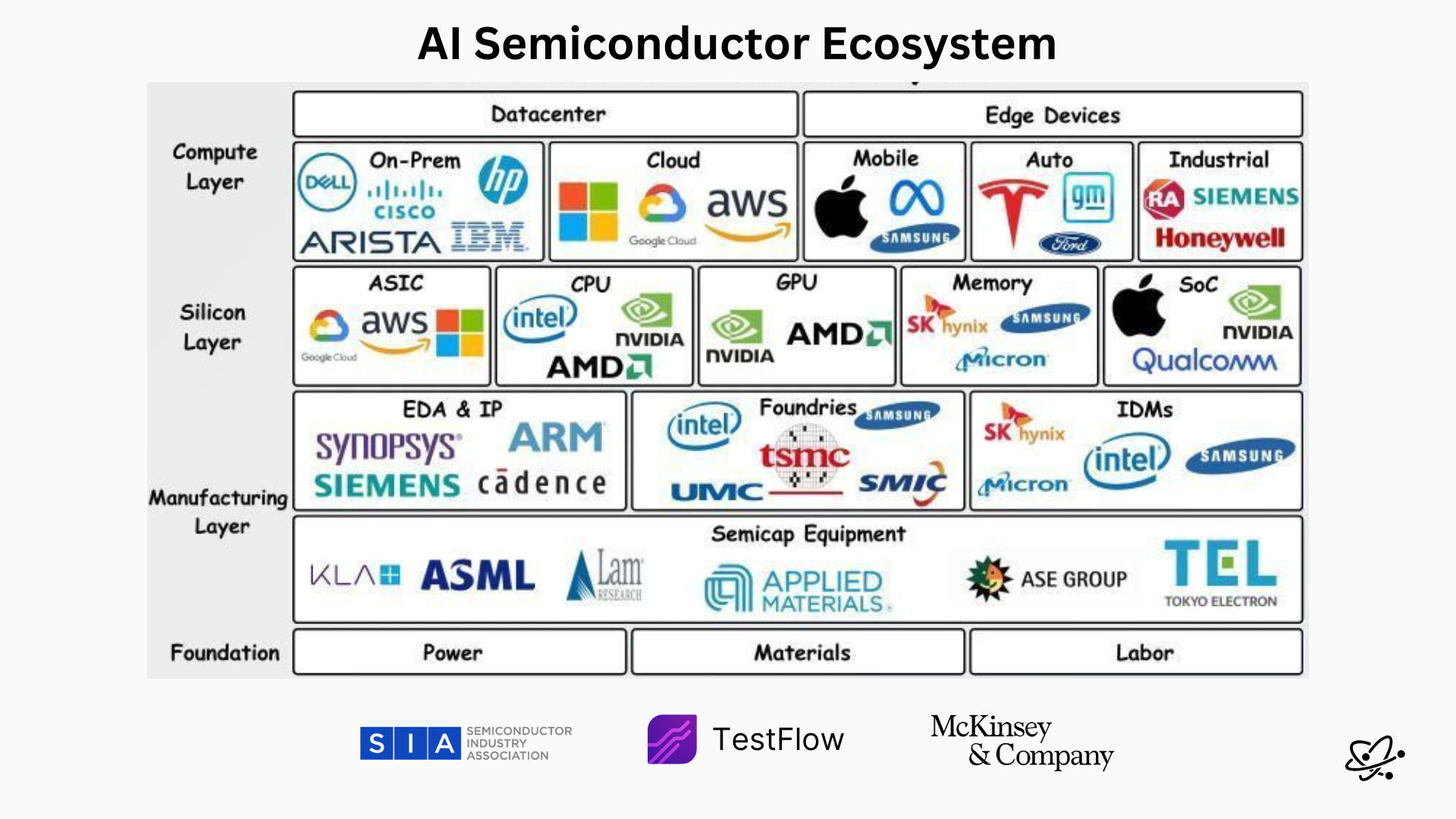
TOKYO / ARMONK — In the high-stakes theater of global geopolitics and advanced hardware engineering, alliances are forged not merely for corporate synergy, but for national economic survival. When International Business Machines Corporation (IBM) and the newly minted Japanese foundry Rapidus Corporation inked a landmark strategic partnership, it signaled a seismic shift in the semiconductor supply chain. This alliance, centered on the transfer and commercialization of pioneering 2-nanometer (nm) gate-all-around (GAA) nanosheet node technology, is more than a commercial agreement. It is an industrial crusade designed to restore Japan’s lost sovereignty in microelectronics and construct an unshakeable technological bulwark against supply chain vulnerabilities in East Asia.
For institutional investors, enterprise tech buyers, and global policymakers, this partnership introduces a dynamic new variable into the valuation multiples and capital allocation strategies of the world's leading technology titans. As enterprise ROI increasingly relies on hyper-specialized accelerators, AI inferencing chips, and hyper-scalable cloud compute architectures, the geopolitical stability of silicon fabrication has never been more paramount. This investigative report dissects the strategic anatomy of the IBM-Rapidus pact, examining the technological imperatives, capital commitments, and macroeconomic repercussions that will define the next decade of enterprise tech infrastructure.
Executive Takeaways
Test Our Free AI & Tech Utilities Suite
Calculate LLM API token costs, analyze article dwell-time, or simulate tech DCA returns.
- 2nm Breakthrough Transfer: IBM is licensing its industry-leading 2nm gate-all-around (GAA) nanosheet process technology to Rapidus, enabling Japan to leapfrog mature nodes and target bleeding-edge manufacturing.
- Sovereign Industrial Policy: Backed by substantial subsidies from the Japanese Ministry of Economy, Trade and Industry (METI), Rapidus represents Tokyo's aggressive bid to re-establish domestic semiconductor manufacturing leadership.
- Ecosystem Co-Development: Beyond pure foundry services, the partnership encompasses joint R&D, talent cultivation, and the creation of an advanced packaging ecosystem anchored in Hokkaido, Japan.
- Geopolitical Risk Mitigation: The alliance serves as a critical risk-mitigation framework, diversifying high-end chip production away from concentrated geographic fault lines and securing resilient supply chains for multinational enterprise clients.
Comprehensive Narrative: The Genesis of an Industrial Alliance

To understand the magnitude of the December 2022 agreement between IBM and Rapidus, one must first examine the historical trajectory of Japan’s semiconductor industry. During the late 20th century, Japanese firms dominated global memory and logic production, capturing over 50 percent of the world market. However, through a combination of shifting macroeconomic tides, fierce competition from South Korean and Taiwanese foundries, and the immense capital expenditures required to keep pace with Moore’s Law, Japan’s advanced manufacturing capacity steadily eroded. By the turn of the decade, domestic fabrication was largely relegated to legacy nodes, leaving Japanese automotive, industrial, and digital infrastructure heavily reliant on foreign foundries.
The catalytic event for change arrived in the wake of post-pandemic supply chain disruptions and escalating geopolitical friction surrounding Taiwan and the South China Sea. Recognizing that hardware dependency is a critical national security vulnerability, the Japanese government mobilized unprecedented capital allocation strategies. METI spearheaded the creation of Rapidus, assembling a consortium of Japan’s most iconic corporate heavyweights—including Toyota, Sony, NTT, SoftBank, Kioxia, Denso, NEC, and MUFG Bank—to pool capital, expertise, and commercial intent.
Simultaneously, IBM had been aggressively advancing its semiconductor research capabilities. At its Albany NanoTech Complex in New York, IBM’s research division achieved a monumental breakthrough in May 2021 by unveiling the world’s first 2nm chip design. By utilizing nanosheet architecture, IBM’s 2nm chips demonstrated the ability to fit 50 billion transistors onto a fingernail-sized die, delivering a 45 percent performance increase or a 75 percent energy-efficiency boost compared to prevailing 7nm node technologies.
However, inventing a breakthrough node in a laboratory setting is vastly different from scaling it to commercial high-volume manufacturing (HVM). This is where the IBM-Rapidus synergy became a masterclass in strategic alignment. Rapidus needed a foundational, world-class technology stack to bypass years of iterative development, while IBM needed a trusted, highly capable manufacturing partner to commercialize its innovations and counter the dominance of overseas foundry monopolies.
Under the terms of the agreement, Rapidus engineers were dispatched directly to the Albany NanoTech Complex to work side-by-side with IBM researchers, absorbing the intricate physics, material science, and process integration required for 2nm GAA fabrication. Simultaneously, Rapidus broke ground on the IIM (Innovative Integration for Manufacture) facility in Chitose, Hokkaido, designed to serve as the crown jewel of Japan's new semiconductor ecosystem.
Verified Data & Metrics Breakdown
| Metric / Specification | IBM / Albany R&D Baseline | Rapidus Target (Hokkaido Facility) | Strategic Impact |
|---|---|---|---|
| Node Technology | 2nm Nanosheet (GAA) | 2nm Nanosheet (GAA) | Bleeding-edge performance for AI & HPC |
| Pilot Line Operational Target | Active (Albany, NY) | Q2 2025 (Chitose, Hokkaido) | Rapid transition from lab to pilot scale |
| Mass Production Target | N/A (R&D Focus) | 2027 | Commercial availability for enterprise clients |
| Initial Government Subsidies | CHIPS Act Alignment | > 330 Billion Yen (~$2.3B+ USD initial) | De-risks capital expenditure for private investors |
| Target Application Markets | Enterprise Servers, Quantum | AI, Autonomous Vehicles, Edge Computing | High-growth sectors demanding extreme efficiency |
Industry & Market Implications
The formation of this alliance sends reverberations across the global technology landscape, fundamentally altering competitive dynamics among enterprise hardware vendors, cloud service providers, and semiconductor foundries.
1. Diversification and Supply Chain Risk Mitigation
For multinational corporations dependent on resilient infrastructure scalability, the over-concentration of advanced foundry capacity in a single geopolitical hotspot has long been an unmitigated enterprise risk. The emergence of Rapidus as a viable, Western-aligned alternative in Japan provides a vital risk-mitigation valve. Enterprise buyers can now architect their next-generation data centers and cloud compute architectures knowing that geopolitical shocks will not instantly paralyze their hardware procurement pipelines.
2. The AI Hardware Boom and Energy Efficiency
As generative artificial intelligence and large language models (LLMs) drive unprecedented demands for computational power, power consumption has emerged as the ultimate operational bottleneck. Data center operators face mounting regulatory compliance pressures and soaring electricity expenditures. The 2nm GAA architecture pioneered by IBM and operationalized by Rapidus offers a transformative solution: dramatic performance gains per watt. This efficiency directly impacts enterprise ROI, lowering the total cost of ownership (TCO) for massive AI model training and inferencing deployments.
3. Competitive Pressures on Incumbent Foundries
While industry giants like TSMC, Samsung, and Intel command the lion's share of global foundry revenues, Rapidus introduces a specialized, high-agility competitor. By focusing aggressively on fast-turnaround prototyping and custom manufacturing for high-value AI and edge-computing applications, Rapidus carves out a lucrative niche. This forces incumbent players to continuously optimize their pricing models, technological roadmaps, and customer service frameworks.
People Also Ask (FAQ)
What is the core objective of the IBM and Rapidus partnership?
The primary objective is to jointly develop and commercialize advanced 2-nanometer gate-all-around (GAA) semiconductor manufacturing technology in Japan. By combining IBM’s groundbreaking research—developed at its Albany NanoTech Complex—with Rapidus' state-of-the-art foundry infrastructure in Hokkaido, the partnership aims to re-establish Japan as a global leader in bleeding-edge microelectronics production and secure resilient supply chains for enterprise tech markets.
How does Rapidus plan to fund its multi-billion dollar foundry operations?
Rapidus utilizes a hybrid funding model combining substantial direct equity investments from Japan's leading industrial enterprises (including Toyota, Sony, NTT, and SoftBank) with massive financial backing and subsidies from the Japanese government via the Ministry of Economy, Trade and Industry (METI). This public-private partnership effectively shares capital expenditure risks, enabling Rapidus to aggressively pursue high-cost advanced node manufacturing.
What makes IBM's 2nm nanosheet technology superior to older nodes?
IBM's 2nm nanosheet architecture allows for an unprecedented density of approximately 50 billion transistors on a chip the size of a fingernail. Compared to standard 7nm chips, this technology delivers up to a 45 percent increase in computational performance or a 75 percent reduction in power consumption. For enterprise data centers and AI workloads, this translates into massive efficiency gains, lower energy costs, and superior processing speeds.
When will Rapidus begin commercial mass production of 2nm chips?
Rapidus established a pilot manufacturing line in Chitose, Hokkaido, slated for initial operations and sample production runs. The strategic roadmap targets full-scale commercial mass production by 2027. This timeline is aggressively compressed compared to traditional foundry development cycles, reflecting the urgent international demand for secure, advanced semiconductor manufacturing capacity.
Future Outlook & Strategic Milestones
As the semiconductor industry navigates the physical limits of silicon scaling, the success of the IBM-Rapidus partnership will serve as a definitive litmus test for sovereign industrial policy and cross-border technological collaboration. The coming 24 to 36 months will be characterized by critical milestones that institutional investors and technology executives must monitor closely:
- Pilot Line Validation (2025): The successful commissioning and yield stabilization of the IIM facility pilot line in Hokkaido will prove whether Rapidus can successfully replicate and scale IBM’s complex 2nm process recipes.
- Customer Adoption and Design Wins: Securing anchor enterprise design wins from global hyperscalers, automotive leaders, and AI accelerator developers will validate the commercial viability of Rapidus' foundry model.
- Next-Generation R&D Expansion: Beyond 2nm, the longevity of the partnership will depend on joint advancements into sub-2nm nodes, backside power delivery networks, and advanced 3D packaging technologies.
In conclusion, the IBM and Rapidus alliance transcends standard corporate deal-making. It is a calculated, well-funded masterstroke that rewrites the geography of advanced manufacturing. For enterprises navigating an era of digital transformation, AI proliferation, and geopolitical uncertainty, this partnership offers a promising horizon: a more resilient, efficient, and diversified global semiconductor ecosystem.